MSM7557 데이터 시트보기 (PDF) - Oki Electric Industry
부품명
상세내역
일치하는 목록
MSM7557 Datasheet PDF : 25 Pages
| |||
¡ Semiconductor
MSM7557
(Continued)
Name
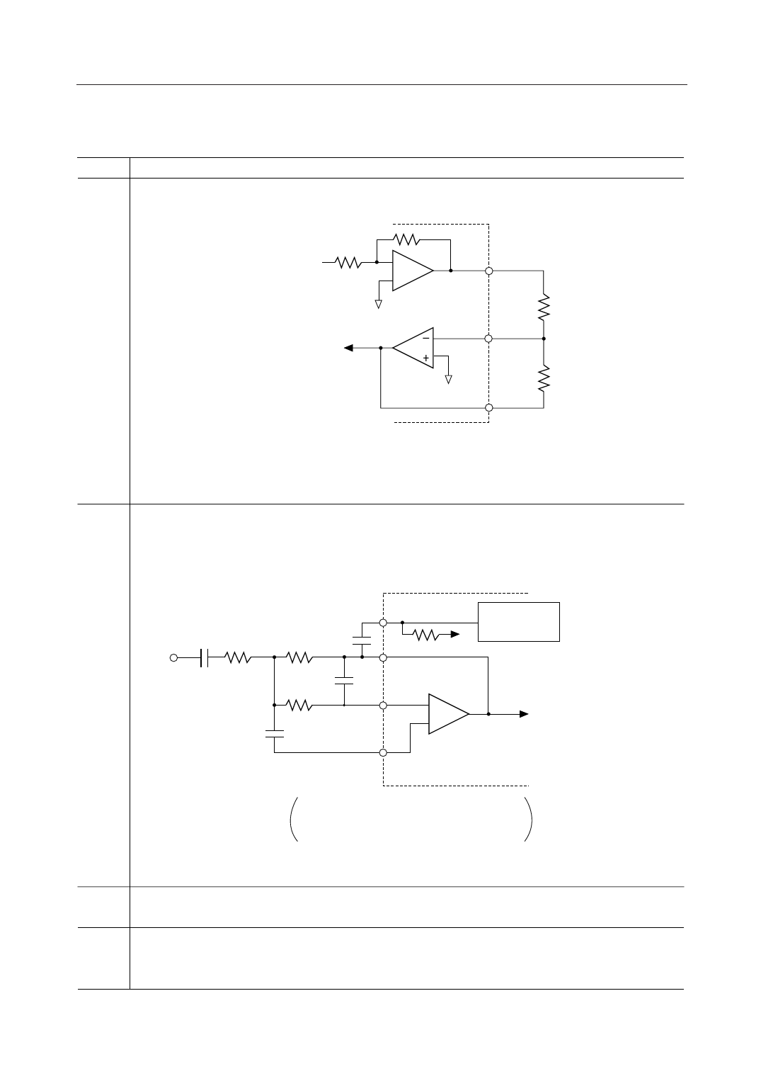
Modulator output level control.
Refer to the following figure.
From modulator
VR1
VR2
To transmit filter
VR3
Description
R1 ≥ 40 kW
R2 ≥ 40 kW
–
VR1
R1 ≥ R2
+
R1
VR2
R2
VR3
VTAO = 20 ¥ log (R2/R1) – 9 dBV (DYN = "0" )
VTAO = 20 ¥ log (R2/R1) – 1 dBV (DYN = "1" )
This level is made from internal voltage reference, so this level doesn't depend on power supply voltage.
Transmit side RC active filter input (TVI) and output (TVIO).
If over 50 kHz frequency element is in the input signal, folding noise is generated from internal SCF
circuit, so second order RC-active filter is needed. (fc = 10 kHz)
TVIO
TVI
C1 R3
C2
C19
R5
C3
R4
CMPI
TVIO
TVI –
+
SG
Compressor
R5 ≥ 60 kW
C1 and C19 are used for DC cut.
VTVI
Example of fc = 10 kHz and 0 dB gain
R3 = R4 = R5 = 68 kW
C1 = 0.22 mF, C2 = 510 pF, C3 = 110 pF
CC1
CC2
CC3N
CC3P
When digital "1" is applied to TVE pin, transmit voice signal comes out to TAO.
Capacitor connection pins to remove for DC offset of the compressor.
A 1 mF capacitor between SG pin and each pin should be connected.
Capacitor connection pins for the compressor attack and recovery time.
When DYN is digital "0" level, a 0.22 mF capacitor should be connected between CC3N and CC3P.
And when DYN is digital "1" level, a 0.47 mF capacitor should be connected between them.
5/25
Share Link: 