MSM7557 데이터 시트보기 (PDF) - Oki Electric Industry
부품명
상세내역
일치하는 목록
MSM7557 Datasheet PDF : 25 Pages
| |||
¡ Semiconductor
MSM7557
PIN DESCRIPTION
Name
Description
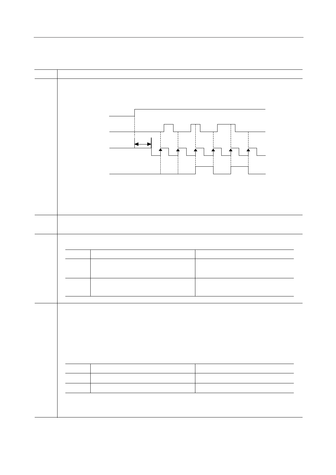
Transmit data input.
The data on SD pin are took into MSK modulator and the data are available on the positive edge of ST.
ME
SD input
tMS
SD
ST
Modulator
input data
In order to synchronize a receive modem, more than 18bits bit-synchronous signal should be
transmitted before data transmission. If S/N ratio of the receive signal is always good, more than
11bits bit-synchronous signal synchronizes the receiver.
Transmit data timing clock output.
ST
When digital "0" is put on ME pin, ST is fixed to digital "1" level.
Emphasis path selection.
EMP
Transmit side
Receive side
EMP
0
Pre-emphasis circuit is bypassed to the De-emphasis circuit is bypassed to the
path
path
Pre-emphasis circuit is connected to the De-emphasis circuit is connected to the
1
path
path
Deviation limiter control.
Voice signal maximum Rf modulation level is controlled by connecting external reference voltage to
this pin.
Input impedance of this pin is about 200 kW.
When this pin is left open, internal reference voltage is used as the clamp level.
LIM Internal clamp level is as follows.
DYN
Internal clamp level
Limiter level
0
0.50 V
–9 dBV
1
1.26 V
–1 dBV
This internal clamp level is made by internal reference voltage which is unrelated with VDD.
Negative clamp level is made by internal operational amplifier and the voltage is reversed at VSG.
4/25
Share Link: 