MC74HCT132A(2016) 데이터 시트보기 (PDF) - ON Semiconductor
부품명
상세내역
일치하는 목록
MC74HCT132A
(Rev.:2016)
(Rev.:2016)
ON Semiconductor

MC74HCT132A Datasheet PDF : 8 Pages
| |||
MC74HCT132A
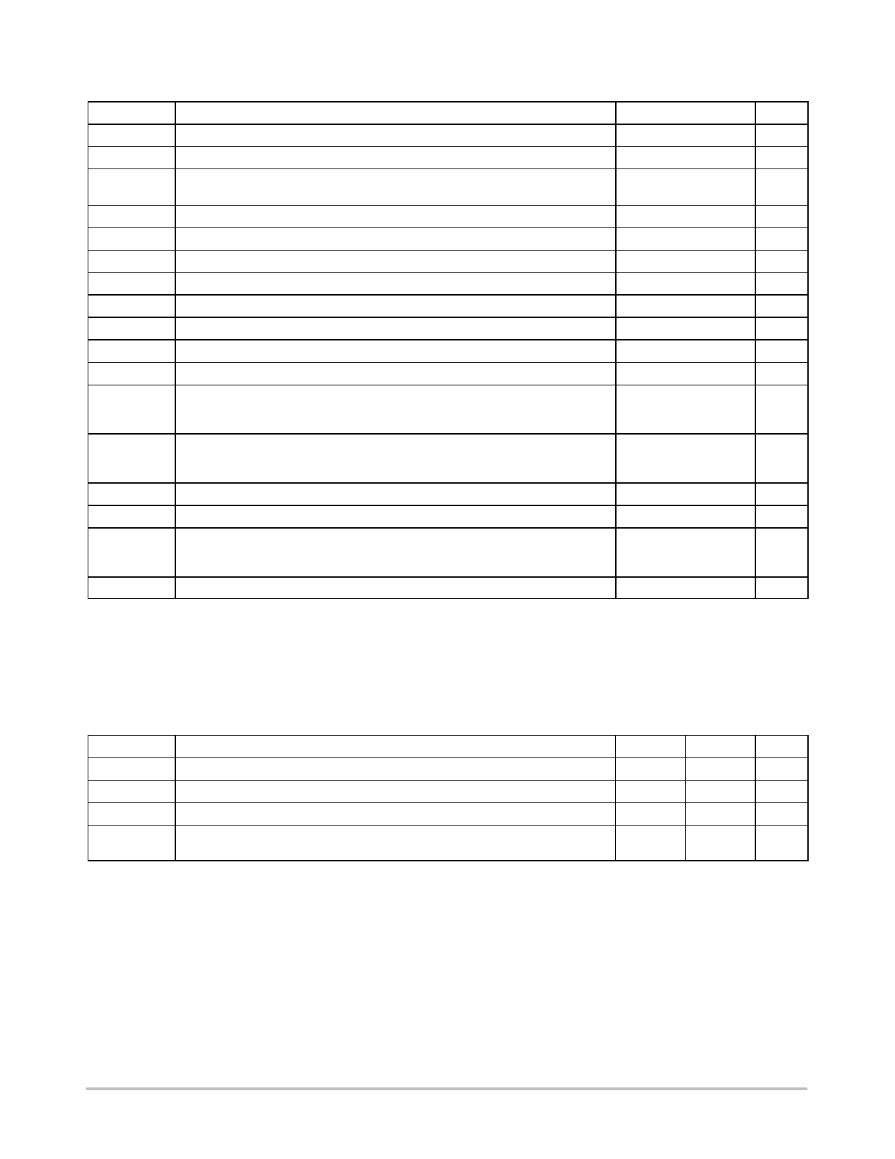
MAXIMUM RATINGS
Symbol
Parameter
Value
Unit
VCC
VIN
VOUT
IIK
IOK
IOUT
ICC
IGND
TSTG
TL
TJ
qJA
Positive DC Supply Voltage
Digital Input Voltage
DC Output Voltage
Input Diode Current
Output Diode Current
DC Output Current, per Pin
DC Supply Current, VCC and GND Pins
DC Ground Current per Ground Pin
Storage Temperature Range
Lead Temperature, 1 mm from Case for 10 Seconds
Junction Temperature Under Bias
Thermal Resistance
Output in 3−State
High or Low State
14−SOIC
14−TSSOP
*0.5 to )7.0
*0.5 to )7.0
*0.5 to )7.0
*0.5 to VCC )0.5
*20
$20
$25
$75
$75
*65 to )150
260
)150
125
170
V
V
V
mA
mA
mA
mA
mA
_C
_C
_C
_C/W
PD
Power Dissipation in Still Air at 85_C
SOIC
500
mW
TSSOP
450
MSL
Moisture Sensitivity
Level 1
FR
VESD
Flammability Rating
ESD Withstand Voltage
Oxygen Index: 30% − 35% UL 94 V0 @ 0.125 in
Human Body Model (Note 1)
u2000
V
Machine Model (Note 2)
u100
Charged Device Model (Note 3)
u500
ILatch−Up
Latch−Up Performance
Above VCC and Below GND at 85_C (Note 4)
$300
mA
Stresses exceeding those listed in the Maximum Ratings table may damage the device. If any of these limits are exceeded, device functionality
should not be assumed, damage may occur and reliability may be affected.
1. Tested to EIA/JESD22−A114−A.
2. Tested to EIA/JESD22−A115−A.
3. Tested to JESD22−C101−A.
4. Tested to EIA/JESD78.
RECOMMENDED OPERATING CONDITIONS
Symbol
Parameter
Min
Max
Unit
VCC
VIN, VOUT
TA
tr, tf
DC Supply Voltage (Referenced to GND)
DC Input Voltage, Output Voltage (Referenced to GND)
Operating Temperature, All Package Types
Input Rise and Fall Time (Figure 3)
2.0
0
*55
−
6.0
V
VCC
V
)125
_C
No Limit
ns
(Note 5)
Functional operation above the stresses listed in the Recommended Operating Ranges is not implied. Extended exposure to stresses beyond
the Recommended Operating Ranges limits may affect device reliability.
5. When VIN X 0.5 VCC, ICC >> quiescent current.
6. Unused inputs may not be left open. All inputs must be tied to a high−logic voltage level or a low−logic input voltage level.
www.onsemi.com
3
Share Link: