MC74HCT132A(2016) 데이터 시트보기 (PDF) - ON Semiconductor
부품명
상세내역
일치하는 목록
MC74HCT132A
(Rev.:2016)
(Rev.:2016)
ON Semiconductor

MC74HCT132A Datasheet PDF : 8 Pages
| |||
MC74HCT132A
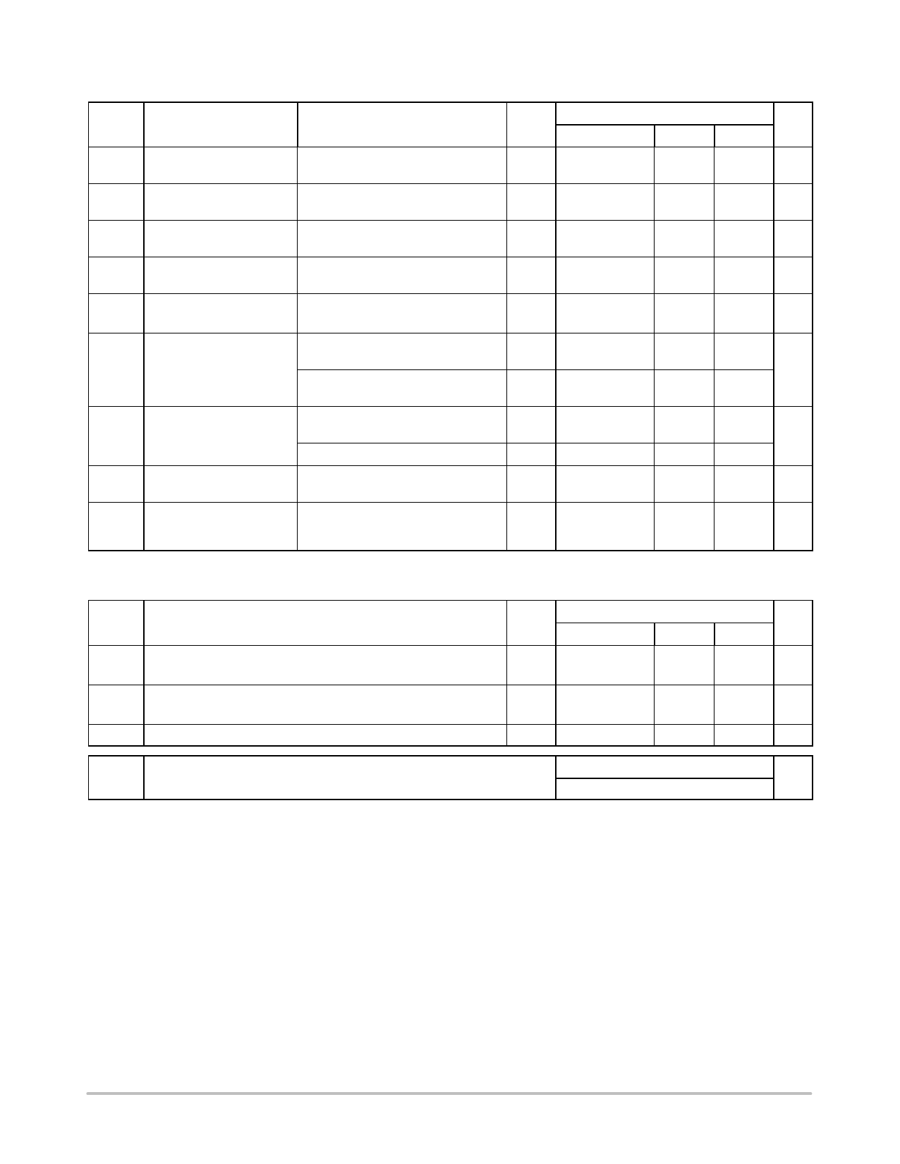
DC ELECTRICAL CHARACTERISTICS (Voltages Referenced to GND)
Symbol
Parameter
VCC
Test Conditions
V
VT+max Maximum Positive−Going VOUT = 0.1 V
4.5
Input Threshold Voltage
|IOUT| v 20 mA
5.5
VT+min Minimum Positive−Going VOUT = 0.1 V
4.5
Input Threshold Voltage
|IOUT| v 20 mA
5.5
VT–max Maximum Negative−Going VOUT = VCC – 0.1 V
4.5
Input Threshold Voltage
|IOUT| v 20 mA
5.5
VT–min Minimum Negative−Going VOUT = VCC – 0.1 V
4.5
Input Threshold Voltage
|IOUT| v 20 mA
5.5
VHmin Minimum Hysteresis
VOUT = 0.1 V or VCC – 0.1 V
4.5
(Note 7) Voltage
|IOUT| v 20 mA
5.5
VOH Minimum High−Level
VIN v VT−min or VT+max
4.5
Output Voltage
|IOUT| v 20 mA
5.5
VIN v −VT−min or VT+max
|IOUT| v 4.0 mA 4.5
VOL Maximum Low−Level
VIN ≥ VT+max
4.5
Output Voltage
|IOUT| v 20 mA
5.5
VIN ≥ VT+max
|IOUT| v 4.0 mA 4.5
IIN
Maximum Input Leakage VIN = VCC or GND
5.5
Current
Guaranteed Limit
*55_C to 25_C v85_C v125_C Unit
1.9
1.9
1.9
V
2.1
2.1
2.1
1.2
1.2
1.2
V
1.4
1.4
1.4
1.2
1.2
1.2
V
1.4
1.4
1.4
0.5
0.5
0.5
V
0.6
0.6
0.6
0.4
0.4
0.4
V
0.4
0.4
0.4
4.4
4.4
4.4
V
5.4
5.4
5.4
3.98
0.1
0.1
0.26
$0.1
3.84
0.1
0.1
0.33
$1.0
3.7
0.1
V
0.1
0.4
$1.0 mA
ICC Maximum Quiescent
Supply Current
(per Package)
VIN = VCC or GND
IOUT = 0 mA
5.5
1.0
10
40
mA
Product parametric performance is indicated in the Electrical Characteristics for the listed test conditions, unless otherwise noted. Product
performance may not be indicated by the Electrical Characteristics if operated under different conditions.
7. VHmin u (VT+min) * (VT−max); VHmax = (VT+max) ) (VT−min).
AC ELECTRICAL CHARACTERISTICS (CL = 50 pF, Input tr = tf = 6.0 ns, VCC = 5.0 V ± 10%)
VCC
Guaranteed Limit
Symbol
Parameter
V *55_C to 25_C v85_C v125_C Unit
tPLH,
tPHL
tTLH,
tTHL
Maximum Propagation Delay, Input A or B to Output Y
(Figures 3 and 4)
Maximum Output Transition Time, Any Output
(Figures 3 and 4)
5.0
25
5.0
15
31
38
ns
19
22
ns
Cin Maximum Input Capacitance
—
10
10
10
pF
Typical @ 25°C, VCC = 5.0 V
CPD Power Dissipation Capacitance (per Gate) (Note 8)
24
pF
8. Used to determine the no−load dynamic power consumption: PD = CPD VCC2f + ICC VCC.
www.onsemi.com
4
Share Link: