MC145540 데이터 시트보기 (PDF) - Motorola => Freescale
부품명
상세내역
일치하는 목록
MC145540 Datasheet PDF : 116 Pages
| |||
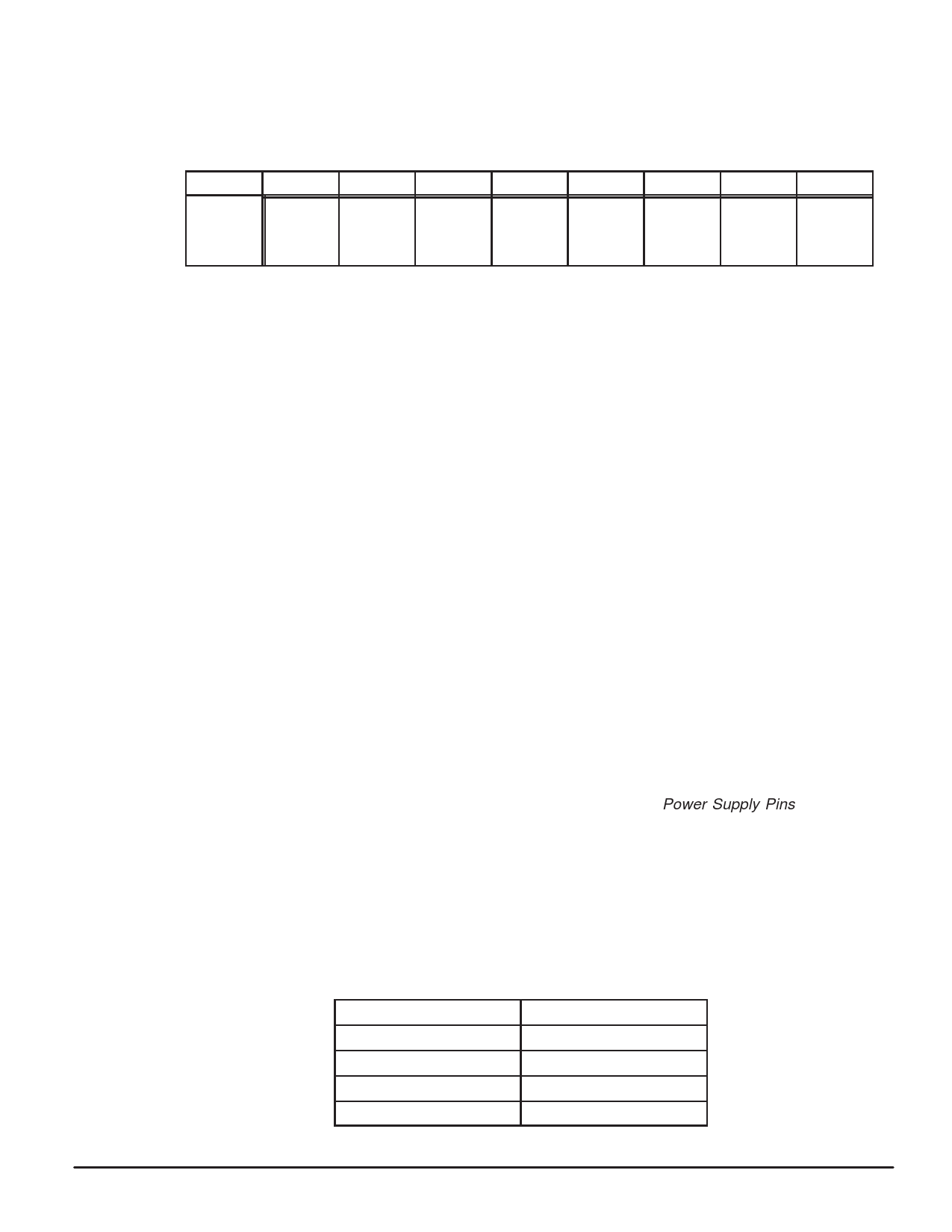
3.4 BYTE REGISTERS
3.4.1 BR0
This register contains several miscellaneous control bits. All bits are cleared on hardware reset, but are
unaffected by a software reset.
BYTE
BR0
b7
b6
b5
b4
b3
EXT
256 kHz
CLK
rw
Mu/A LAW
SELECT
ANALOG
LOOPBACK
rw
rw
I/O MODE
(1)
rw
I/O MODE
(0)
rw
b2
CHARGE
PUMP
DISABLE
rw
b1
ANALOG
POWER
DOWN
rw
b0
DIGITAL
POWER
DOWN
rw
External 256 kHz Clock — This bit controls a mux that selects between an internal or external 256 kHz
signal for clocking the PCM Codec block. When this bit is cleared the mux will select the 256 kHz clock
from the internal clock generator block. When this bit is set, BCLKR is used to provide an external
256 kHz signal and the internal BCLKR signal will then be supplied from BCLKT.
Mu/A Law Select — This bit controls the compression for the encoder and the expansion for the decod-
er. Clearing this bit selects Mu-Law companding of the PCM data. Setting this bit selects A-Law com-
panding of the PCM data.
Analog Loopback — Setting this bit enables the user to perform an Analog Loopback from the receive
path to the transmit path. Internally the signal at the RO output is routed through an analog switch to the
stage of the transmit path between the output of the TG op amp and the input to the transmit trim gain
circuitry. The output of the TG op amp is disconnected from this node.
I/O Mode (1:0) — These bits are used to configure the MC145540 for different modes of operation and
test (see Table 3-3). Two of the modes select whether the device will function as a combined ADPCM
Codec (I/O Mode 00) or as a PCM Codec (I/O Mode 01). The third mode (I/O Mode 10) accommodates
independent access to the output of the PCM A/D and the input to the ADPCM encoder. This permits the
CCITT/ANSI ADPCM encoder and decoder test vectors to be run, as well as allowing for applications
where the PCM data from the A/D may need to be externally processed before being encoded by the
ADPCM encoder. The last mode (I/O Mode 11) allows the user to perform a battery test, effectively
sampling the voltage present at the VEXT pin. In this mode, the ADC is programmed to output a linear
8-bit PCM word for the voltage at VEXT which is intended to be read in BR9 (b7:b0). The data format for
the ADC output is the sign bit and seven magnitude bits. The sign bit is a “don’t care.” The scaling for the
ADC is for 6.3 V at VEXT equals full scale (BIN X111 1111). The ADPCM algorithm does not support dc
signals.
Charge Pump Disable — Setting this bit disables the operation of the charge pump circuitry, which
normally provides a charge pumped 5 V supply (derived from the VEXT external supply) to the VDD pin,
which is also the power supply input for the analog blocks of the device. Disabling the charge pump will
internally connect the VDD pin to the VEXT pin. See Section 2.4.1, Power Supply Pins, for further
information.
Analog Power Down — When set, this bit forces a power down of the PCM Codec block and the
charge pump. This causes the chip to enter a mode in which all clocks to the analog blocks are halted.
This bit must be cleared before the PCM Codec block can function in its normal mode.
Digital Power Down — When set, this bit forces all clocks to the DSP Engine block to be halted. Clear-
ing this bit will force the DSP Engine to come out of power down and execute an initialization procedure
before starting to execute the ADPCM algorithm.
Table 3-3. Input/Output Modes
I/O Mode (1:0)
00
01
10
11
MC145540 Mode
ADPCM Codec
PCM Codec
CCITT Test
Battery Test
MOTOROLA
MC145540
3-3
Share Link: 