MC14017B 데이터 시트보기 (PDF) - Motorola => Freescale
부품명
상세내역
일치하는 목록
MC14017B Datasheet PDF : 7 Pages
| |||
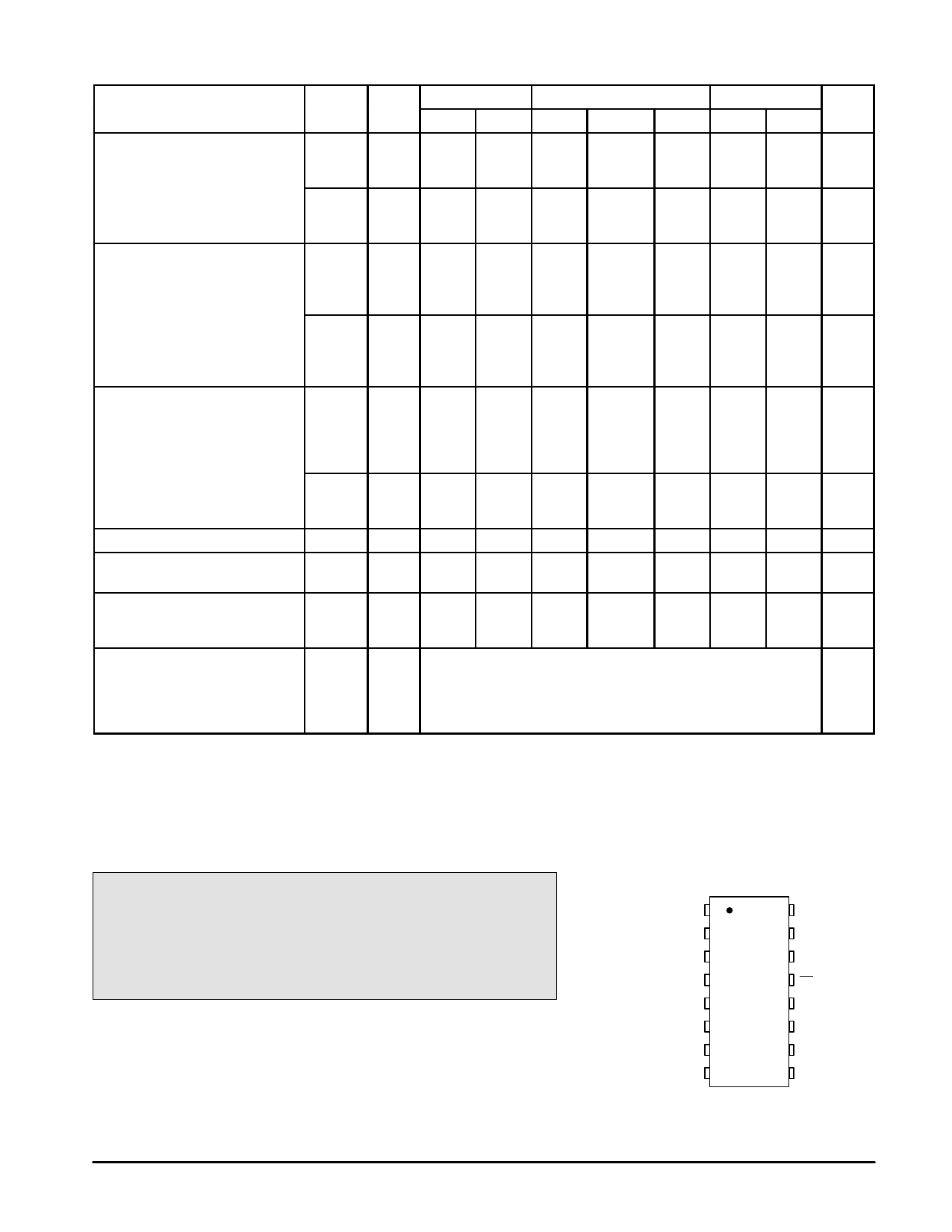
ÎÎÎÎÎÎÎÎÎÎÎÎÎÎÎÎÎÎÎÎÎÎÎÎÎÎÎÎÎÎÎÎÎÎÎÎÎÎÎÎÎÎÎÎÎÎÎÎÎÎÎÎÎÎÎÎÎÎÎÎÎÎÎÎÎÎÎÎÎÎÎÎÎÎÎÎÎÎÎÎÎÎÎÎÎÎÎÎÎÎÎÎÎÎÎÎÎÎÎÎÎÎ ELECTRICAL CHARACTERISTICS (Voltages Referenced to VSS)
ÎÎÎÎÎÎÎÎÎÎÎÎÎÎÎÎÎÎÎÎÎÎÎÎÎÎÎÎÎÎÎÎÎÎÎÎÎÎÎÎÎÎÎÎÎÎÎÎÎÎÎÎÎÎÎÎÎÎÎÎÎÎÎÎÎÎÎÎ Characteristic
VDD
Symbol Vdc
– 55_C
Min
Max
ÎÎÎÎÎÎÎÎÎÎÎÎÎÎÎÎÎÎÎÎÎÎÎÎÎÎÎÎÎÎÎÎÎÎ Output Voltage
ÎÎÎÎÎÎÎÎÎÎÎÎÎÎÎÎÎÎÎÎÎÎÎÎÎÎÎÎÎÎÎÎÎÎ Vin = VDD or 0
“0” Level VOL
5.0
—
0.05
10
—
0.05
15
—
0.05
ÎÎÎÎÎÎÎÎÎÎÎÎÎÎÎÎÎÎÎÎÎÎÎÎÎÎÎÎÎÎÎÎÎÎÎÎÎÎÎÎÎÎÎÎÎÎÎÎÎÎÎÎÎÎÎÎÎÎÎÎÎÎÎÎÎÎÎÎ Vin = 0 or VDD
“1” Level VOH
5.0
4.95
—
10
9.95
—
15
14.95
—
ÎÎÎÎÎÎÎÎÎÎÎÎÎÎÎÎÎÎÎÎÎÎÎÎÎÎÎÎÎÎÎÎÎÎÎÎÎÎÎÎÎÎÎÎÎÎÎÎÎÎÎÎÎÎÎÎÎÎÎÎÎÎÎÎÎÎÎÎ Input Voltage
“0” Level VIL
(VO = 4.5 or 0.5 Vdc)
5.0
—
1.5
ÎÎÎÎÎÎÎÎÎÎÎÎÎÎÎÎÎÎÎÎÎÎÎÎÎÎÎÎÎÎÎÎÎÎ (VO = 9.0 or 1.0 Vdc)
10
—
3.0
(VO = 13.5 or 1.5 Vdc)
15
—
4.0
ÎÎÎÎÎÎÎÎÎÎÎÎÎÎÎÎÎÎÎÎÎÎÎÎÎÎÎÎÎÎÎÎÎÎÎÎÎÎÎÎÎÎÎÎÎÎÎÎÎÎÎÎÎÎÎÎÎÎÎÎÎÎÎÎÎÎÎÎ “1”Level VIH
(VO = 0.5 or 4.5 Vdc)
5.0
3.5
—
ÎÎÎÎÎÎÎÎÎÎÎÎÎÎÎÎÎÎÎÎÎÎÎÎÎÎÎÎÎÎÎÎÎÎ (VO = 1.0 or 9.0 Vdc)
10
7.0
—
(VO = 1.5 or 13.5 Vdc)
15
11
—
ÎÎÎÎÎÎÎÎÎÎÎÎÎÎÎÎÎÎÎÎÎÎÎÎÎÎÎÎÎÎÎÎÎÎ Output Drive Current
ÎÎÎÎÎÎÎÎÎÎÎÎÎÎÎÎÎÎÎÎÎÎÎÎÎÎÎÎÎÎÎÎÎÎ (VOH = 2.5 Vdc)
ÎÎÎÎÎÎÎÎÎÎÎÎÎÎÎÎÎÎÎÎÎÎÎÎÎÎÎÎÎÎÎÎÎÎ (VOH = 4.6 Vdc)
(VOH = 9.5 Vdc)
ÎÎÎÎÎÎÎÎÎÎÎÎÎÎÎÎÎÎÎÎÎÎÎÎÎÎÎÎÎÎÎÎÎÎ (VOH = 13.5 Vdc)
ÎÎÎÎÎÎÎÎÎÎÎÎÎÎÎÎÎÎÎÎÎÎÎÎÎÎÎÎÎÎÎÎÎÎ (VOL = 0.4 Vdc)
ÎÎÎÎÎÎÎÎÎÎÎÎÎÎÎÎÎÎÎÎÎÎÎÎÎÎÎÎÎÎÎÎÎÎ (VOL = 0.5 Vdc)
(VOL = 1.5 Vdc)
ÎÎÎÎÎÎÎÎÎÎÎÎÎÎÎÎÎÎÎÎÎÎÎÎÎÎÎÎÎÎÎÎÎÎ Input Current
ÎÎÎÎÎÎÎÎÎÎÎÎÎÎÎÎÎÎÎÎÎÎÎÎÎÎÎÎÎÎÎÎÎÎ Input Capacitance
ÎÎÎÎÎÎÎÎÎÎÎÎÎÎÎÎÎÎÎÎÎÎÎÎÎÎÎÎÎÎÎÎÎÎ (Vin = 0)
IOH
Source
Sink IOL
Iin
Cin
5.0 – 3.0
—
5.0 – 0.64
—
10
– 1.6
—
15
– 4.2
—
5.0
0.64
—
10
1.6
—
15
4.2
—
15
—
± 0.1
—
—
—
ÎÎÎÎÎÎÎÎÎÎÎÎÎÎÎÎÎÎÎÎÎÎÎÎÎÎÎÎÎÎÎÎÎÎ Quiescent Current
ÎÎÎÎÎÎÎÎÎÎÎÎÎÎÎÎÎÎÎÎÎÎÎÎÎÎÎÎÎÎÎÎÎÎ (Per Package)
IDD
5.0
—
5.0
10
—
10
15
—
20
ÎÎÎÎÎÎÎÎÎÎÎÎÎÎÎÎÎÎÎÎÎÎÎÎÎÎÎÎÎÎÎÎÎÎ Total Supply Current**†
ÎÎÎÎÎÎÎÎÎÎÎÎÎÎÎÎÎÎÎÎÎÎÎÎÎÎÎÎÎÎÎÎÎÎ (Dynamic plus Quiescent,
ÎÎÎÎÎÎÎÎÎÎÎÎÎÎÎÎÎÎÎÎÎÎÎÎÎÎÎÎÎÎÎÎÎÎ Per Package)
(CL = 50 pF on all outputs, all
ÎÎÎÎÎÎÎÎÎÎÎÎÎÎÎÎÎÎÎÎÎÎÎÎÎÎÎÎÎÎÎÎÎÎÎÎÎÎÎÎÎÎÎÎÎÎÎÎÎÎÎÎÎÎÎÎÎÎÎÎÎÎÎÎÎÎÎÎ buffers switching)
IT
5.0
10
15
25_C
Min
Typ #
Max
—
0
0.05
—
0
0.05
—
0
0.05
4.95
5.0
—
9.95
10
—
14.95
15
—
—
2.25
1.5
—
4.50
3.0
—
6.75
4.0
3.5
2.75
—
7.0
5.50
—
11
8.25
—
– 2.4
– 0.51
– 1.3
– 3.4
– 4.2
– 0.88
– 2.25
– 8.8
0.51
0.88
1.3
2.25
3.4
8.8
— ± 0.00001
—
5.0
—
—
—
—
—
—
—
± 0.1
7.5
—
0.005
5.0
—
0.010
10
—
0.015
20
IT = (0.27 µA/kHz) f + IDD
IT = (0.55 µA/kHz) f + IDD
IT = (0.83 µA/kHz) f + IDD
125_C
Min
Max
—
0.05
—
0.05
—
0.05
4.95
—
9.95
—
14.95
—
—
1.5
—
3.0
—
4.0
3.5
—
7.0
—
11
—
– 1.7
– 0.36
– 0.9
– 2.4
0.36
0.9
2.4
—
—
—
—
—
—
—
—
—
± 1.0
—
—
150
—
300
—
600
Unit
Vdc
Vdc
Vdc
Vdc
mAdc
mAdc
µAdc
pF
µAdc
µAdc
#Data labelled “Typ” is not to be used for design purposes but is intended as an indication of the IC’s potential performance.
** The formulas given are for the typical characteristics only at 25_C.
†To calculate total supply current at loads other than 50 pF:
IT(CL) = IT(50 pF) + (CL – 50) Vfk
where: IT is in µA (per package), CL in pF, V = (VDD – VSS) in volts, f in kHz is input frequency, and k = 0.0011.
This device contains protection circuitry to guard against damage
due to high static voltages or electric fields. However, precautions must
be taken to avoid applications of any voltage higher than maximum rated
voltages to this high-impedance circuit. For proper operation, Vin and
Vout should be constrained to the range VSS ≤ (Vin or Vout) ≤ VDD.
Unused inputs must always be tied to an appropriate logic voltage
level (e.g., either VSS or VDD). Unused outputs must be left open.
PIN ASSIGNMENT
Q5 1
Q1 2
Q0 3
Q2 4
Q6 5
Q7 6
Q3 7
VSS 8
16 VDD
15 RESET
14 CLOCK
13 CE
12 Cout
11 Q9
10 Q4
9 Q8
MOTOROLA CMOS LOGIC DATA
MC14017B
75
Share Link: 