MC14017B 데이터 시트보기 (PDF) - Motorola => Freescale
부품명
상세내역
일치하는 목록
MC14017B Datasheet PDF : 7 Pages
| |||
MOTOROLA
SEMICONDUCTOR TECHNICAL DATA
Decade Counter
The MC14017B is a five–stage Johnson decade counter with built–in code
converter. High speed operation and spike–free outputs are obtained by use
of a Johnson decade counter design. The ten decoded outputs are normally
low, and go high only at their appropriate decimal time period. The output
changes occur on the positive–going edge of the clock pulse. This part can
be used in frequency division applications as well as decade counter or
decimal decode display applications.
• Fully Static Operation
• DC Clock Input Circuit Allows Slow Rise Times
• Carry Out Output for Cascading
• Divide–by–N Counting
• Supply Voltage Range = 3.0 Vdc to 18 Vdc
• Capable of Driving Two Low–power TTL Loads or One Low–power
Schottky TTL Load Over the Rated Temperature Range
• Pin–for–Pin Replacement for CD4017B
ÎÎÎÎÎÎÎÎÎÎÎÎÎÎÎÎÎÎÎÎÎ • Triple Diode Protection on All Inputs
ÎÎÎÎÎÎÎÎÎÎÎÎÎÎÎÎÎÎÎÎÎÎÎÎÎÎÎÎÎÎÎÎÎÎÎÎÎÎÎÎÎÎ MAXIMUM RATINGS* (Voltages Referenced to VSS)
Symbol
Parameter
Value
Unit
ÎÎÎÎÎÎÎÎÎÎÎÎÎÎÎÎÎÎÎÎÎÎÎÎÎÎÎÎÎÎÎÎÎÎÎÎÎÎÎÎÎÎ VDD DCSupplyVoltage
– 0.5 to + 18.0
V
ÎÎÎÎÎÎÎÎÎÎÎÎÎÎÎÎÎÎÎÎÎ Vin, Vout Input or Output Voltage (DC or Transient) – 0.5 to VDD + 0.5 V
ÎÎÎÎÎÎÎÎÎÎÎÎÎÎÎÎÎÎÎÎÎ lin, lout Input or Output Current (DC or Transient),
± 10
mA
per Pin
ÎÎÎÎÎÎÎÎÎÎÎÎÎÎÎÎÎÎÎÎÎ PD Power Dissipation, per Package†
ÎÎÎÎÎÎÎÎÎÎÎÎÎÎÎÎÎÎÎÎÎ Tstg Storage Temperature
ÎÎÎÎÎÎÎÎÎÎÎÎÎÎÎÎÎÎÎÎÎÎÎÎÎÎÎÎÎÎÎÎÎÎÎÎÎÎÎÎÎÎ TL
Lead Temperature (8–Second Soldering)
500
mW
– 65 to + 150
_C
260
_C
* Maximum Ratings are those values beyond which damage to the device may occur.
†Temperature Derating:
Plastic “P and D/DW” Packages: – 7.0 mW/_C From 65_C To 125_C
Ceramic “L” Packages: – 12 mW/_C From 100_C To 125_C
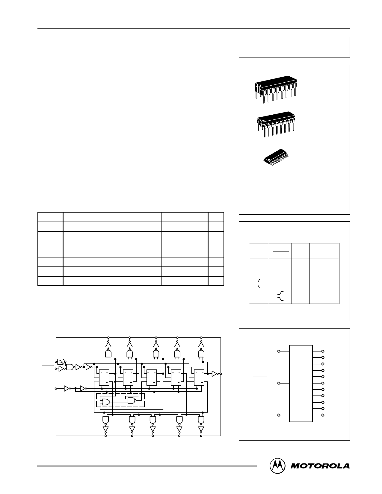
LOGIC DIAGRAM
Q5
Q1
1
2
Q7
Q3
Q9
6
7
11
14
CLOCK
CLOCK
ENABLE 13
15
RESET
CQ
C
DQ
RR
CQ
C
DQ
RR
CQ
C
DQ
RR
CQ
C
DQ
RR
CQ
C
DQ
RR
12
CARRY
REV 3
1/94
©MMCot1or4o0la1, I7nBc. 1995
74
3
5
4
9
10
Q0
Q6
Q2
Q3
Q4
MC14017B
L SUFFIX
CERAMIC
CASE 620
P SUFFIX
PLASTIC
CASE 648
D SUFFIX
SOIC
CASE 751B
ORDERING INFORMATION
MC14XXXBCP
MC14XXXBCL
MC14XXXBD
Plastic
Ceramic
SOIC
TA = – 55° to 125°C for all packages.
FUNCTIONAL TRUTH TABLE
(Positive Logic)
Clock
Decode
Clock Enable Reset Output=n
0
X
0
n
X
1
0
n
X
X
1
Q0
0
0
n+1
X
0
n
X
0
n
1
0
n+1
X = Don’t Care. If n < 5 Carry = “1”,
Otherwise = “0”.
BLOCK DIAGRAM
CLOCK 14
CLOCK
ENABLE 13
RESET 15
Q0
3
Q1
2
Q2
4
Q3
7
Q4
10
Q5
1
Q6
5
Q7
6
Q8
9
Q9
11
Cout
12
VDD = PIN 16
VSS = PIN 8
MOTOROLA CMOS LOGIC DATA
Share Link: 