MC100E211 데이터 시트보기 (PDF) - ON Semiconductor
부품명
상세내역
일치하는 목록
MC100E211 Datasheet PDF : 11 Pages
| |||
MC10E211, MC100E211
APPLICATIONS INFORMATION
General Description
The MC10E/100E211 is a 1:6 fanout tree designed
explicitly for low skew high speed clock distribution. The
device was targeted to work in conjunction with the E111
device to provide another level of flexibility in the design
and implementation of clock distribution trees. The
individual synchronous enable controls and multiplexed
clock inputs make the device ideal as the first level
distribution unit in a distribution tree. The device provides
the ability to distribute a lower speed scan or test clock along
with the high speed system clock to ease the design of system
diagnostics and self test procedures. The individual enables
could be used to allow for the disabling of individual cards
on a backplane in fault tolerant designs.
Because of lower fanout and larger skews the E211 will
not likely be used as an alternative to the E111 for the bulk
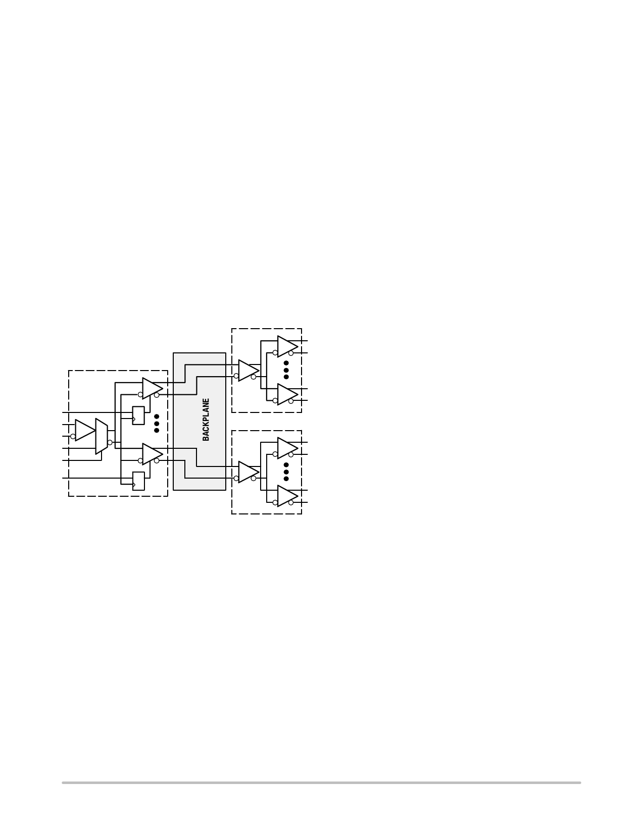
of the clock fanout generation. Figure 3 shows a typical
application combining the two devices to take advantage of
the strengths of each.
E111
Q0
E211
Q0
Q8
E111
Q0
Q5
Q8
Figure 3. Standard E211 Application
Using the E211 in PECL Designs
The E211 device can be utilized very effectively in
designs utilizing only a +5 V power supply. Since the
internal switching reference levels are biased off of the VCC
supply the input thresholds for the single−ended inputs will
vary with VCC. As a result the single−ended inputs should be
driven by a device on the same board as the E211. Driving
these inputs across a backplane where significant
differences between the VCC’s of the transmitter and
receiver can occur can lead to AC performance and/or
significant noise margin degradations. Because the
differential I/O does not use a switching reference, and due
to the CMR range of the E211, even under worst case VCC
situations between cards there will be no AC performance or
noise margin loss for the differential CLK inputs.
For situations where TTL clocks are required the E211 can
be interfaced with the H641 or H643 ECL to TTL Clock
Distribution Chips. The H641 is a single supply 1:9 PECL
to TTL device while the H643 is a 1:8 dual supply standard
ECL to TTL device. By combining the superior skew
performance of the E211, or E111, with the low skew
translating capabilities of the H641 and H643 very low skew
TTL clock distribution networks can be realized.
Handling Open Inputs and Outputs
All of the input pins of the E211 have a 50 kW to 75 kW
pulldown resistor to pull the input to VEE when left open.
This feature can cause a problem if the differential clock
inputs are left open as the input gate current source transistor
will become saturated. Under these conditions the outputs of
the CLK input buffer will go to an undefined state. It is
recommended, if possible,that the SCLK input should be
selected any time the differential CLK inputs are allowed to
float. The SCLK buffer, under open input conditions, will
maintain a defined output state and thus the Q outputs of the
device will be in a defined state (Q = LOW). Note that if all
of the inputs are left open the differential CLK input will be
selected and the state of the Q outputs will be undefined.
With the simultaneous switching characteristics and the
tight skew specifications of the E211 the handling of the
unused outputs becomes critical. To minimize the noise
generated on the die all outputs should be terminated in
pairs, i.e. both the true and complement outputs should be
terminated even if only one of the outputs will be used in the
system. With both complementary pairs terminated the
current in the VCC pins will remain essentially constant and
thus inductance induced voltage glitches on VCC will not
occur. VCC glitches will result in distorted output
waveforms and degradations in the skew performance of the
device.
The package parasitics of the PLCC−28 cause the signals
on a given pin to be influenced by signals on adjacent pins.
The E211 is characterized and tested with all of the outputs
switching, therefore the numbers in the data book are
guaranteed only for this situation. If all of the outputs of the
E211 are not needed and there is a desire to save power the
unused output pairs can be left unterminated. Unterminated
outputs can influence the propagation delay on adjacent pins
by 15 ps − 20 ps. Therefore under these conditions this 15 ps
− 20 ps needs to be added to the overall skew of the device.
Pins which are separated by a package corner are not
considered adjacent pins in the context of propagation delay
influence. Therefore as long as all of the outputs on a single
side of the package are terminated the specification limits in
the data sheet will apply.
http://onsemi.com
7
Share Link: 