M37640E8FP 데이터 시트보기 (PDF) - Mitsumi
부품명
상세내역
일치하는 목록
M37640E8FP Datasheet PDF : 96 Pages
| |||
Ver 1.4
MITSUBISHI MICROCOMPUTERS
7640 Group
SINGLE-CHIP 8-BIT CMOS MICROCOMPUTER
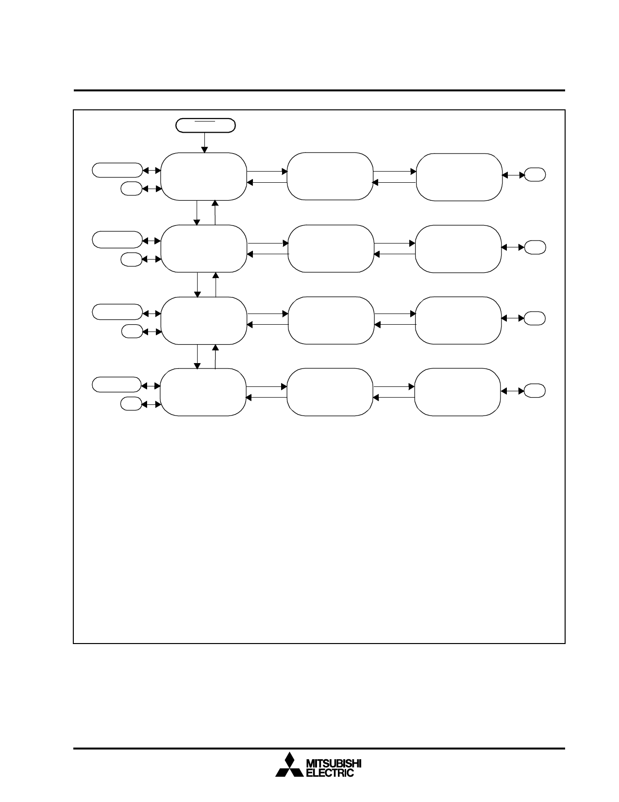
RESET
Xin clock on
FSC0
Xin clock on
CPMA6
Xin clock on
Stop Note 1
Wait
XCin clock stopped
PLL clock stopped
Φ=f(Xin)/4 Note 2
CPMA=0C, FSC=60
1
XCin clock stopped
0
PLL clock on Note 3
Φ=f(Xin)/4 Note 2
CPMA=0C FSC=41
1
XCin clock stopped
0
PLL clock on
Φ=f(PLL)/2
CPMA=4C, FSC=41
Wait
10
CPMA4
Stop Note 1
Xin clock on
XCin clock on
FSC0
1
Xin clock on
XCin clock on
CPMA6
1
Xin clock on
XCin clock on
Wait
PLL clock stopped
Φ=f(Xin)/4 Note 2
CPMA=1C, FSC=60
0
PLL clock on Note 3
Φ=f(Xin)/4 Note 2
CPMA=1C, FSC=41
0
PLL clock on
Φ=f(PLL)/2
CPMA=5C, FSC=41
Wait
10
CPMA7
Stop Note 1
Xin clock on
XCin clock on
FSC0
1
Xin clock on
XCin clock on
CPMA6
1
Xin clock on
XCin clock on
Wait
PLL clock stopped
Φ=f(XCin)/2
CPMA=9C, FSC=60
0
PLL clock on Note 3
Φ=f(XCin)/2
CPMA=9C, FSC=41
0
PLL clock on
Φ=f(PLL)/2
CPMA=DC, FSC=41
Wait
10
CPMA5 Note 4
Xin clock stopped
FSC0
Xin clock stopped
CPMA6
Xin clock stopped
Stop Note 1
XCin clock on
1
XCin clock on
1
XCin clock on
Wait
PLL clock stopped
Φ=f(XCin)/2
CPMA=BC, FSC=68
0
PLL clock on Note 3
Φ=f(XCin)/2
CPMA7=BC, FSC=49
0
PLL clock on
Φ=f(PLL)/2
CPMA7=FC, FSC=49
Wait
Note 1:
Stop mode stops the oscillators that are also the inputs to the frequency synthesizer. However, the
frequency synthesizer is not disabled and so its output is unstable. So, always set the system clock
to an external oscillator and disable the frequency synthesizer before entering stop mode.
Note 2: . = f(Xin)/4 can be interchanged with. = f(Xin)/2 by setting CCR7 to “1”. The same flow chart applies to both
cases.
Note 3:
The input to the frequency synthesizer is independent of the system clock. It can be either Xin or XCin depend
ing on bit 3 of FSC. In the above flow, the input has been chosen to be the same as the system clock only for
simplicity. The oscillator selected to be the input to the frequency synthesizer must be enable before the
frequency synthesizer is enabled.
Note 4: The input clock for the frequency synthesizer must be set to XCin by setting FIN (bit 3 of FSC) to a "1" before
Xin oscillation can be disabled.
Note: CPMA values shown assume single-chip mode with stack in one page.
Fig. 1.90. Clock Flow Diagram
73
Share Link: 