M37640E8FP 데이터 시트보기 (PDF) - Mitsumi
부품명
상세내역
일치하는 목록
M37640E8FP Datasheet PDF : 96 Pages
| |||
Ver 1.4
MITSUBISHI MICROCOMPUTERS
7640 Group
SINGLE-CHIP 8-BIT CMOS MICROCOMPUTER
1.24 OSCILLATOR CIRCUIT
An on-chip oscillator provides the system and periph-
eral clocks as well as the USB clock necessary for
operation. This oscillator circuit is comprised of ampli-
fiers that provide the gain necessary for oscillation,
oscillation control logic, a frequency synthesizer, and
buffering of the clock signals.
A Clock Control register (CCR) is shown in Figure 1.89
and a flow diagram for the oscillator circuit is shown in
Figure 1.90.
The following external clock inputs are supported:
• A quartz crystal oscillator of up to 24 MHz, connected
to the Xin and Xout pins.
• A ceramic resonator or quartz crystal oscillator of
32.768 kHz, connected to the XCin and XCout pins.
• An external clock signal of up to 5.00 MHz, connected
to the XCin pin.
The frequency synthesizer can be used to generate a
48MHz clock signal (fUSB) needed by the USB block
and clock fSYN, which can be chosen as the source
for the system and peripheral clocks. Both fUSB and
fSYN are phase-locked frequency multiples of the fre-
quency synthesizer input. The inputs to the frequency
synthesizer can be either Xin or XCin.
The two-phase non-overlapping system clock (CPU
and peripherals) is derived from the source to the
clock circuit and is half the frequency of the source.
(i.e. Source = 24 MHz, system clock = 12 MHz) Any
one of four clock signals can be chosen as the source
for the system and peripheral clocks; f(Xin)/2, f(Xin),
f(XCin), or fSYN. The selection is based on the values of
bits CPMA6, CPMA7 and CCR7. The default source
after reset is fXin/2.
The default source for the system and peripheral
clocks is f(Xin)/2. If f(Xin)= 24MHz, then the CPU will
be running at F = 6MHz (low frequency mode. For the
CPU to run in high frequency mode, i.e., source of
clock = f(Xin), write a “1” to bit 7 of the clock control
register. (If an external clock signal is input to Xin or
XCin, the inverting amplifiers can be disabled by
means of the CCR6 and CCR7 bits, respectively, in or-
der to reduce power consumption).
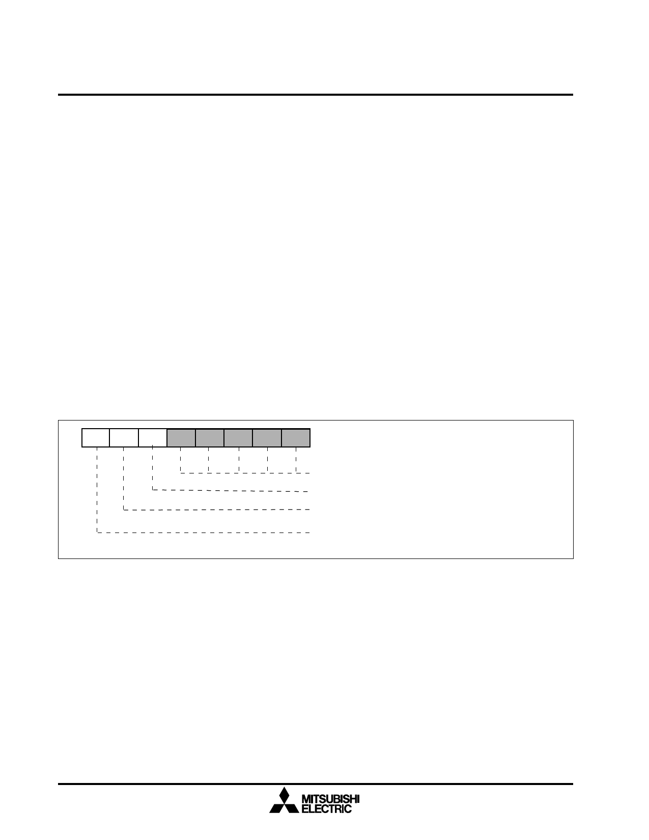
MSB
7
CCR7
CCR6
CCR5
Reserved
Reserved
Reserved
Reserved
Reserved
LSB
0
Address: 001F16
Access: R/W
Reset: 0016
Fig. 1.89. Clock Control Register (CCR)
Bits 0-4
CCR5:
CCR6:
CCR7:
Reserved (Read/Write “0”)
XCout Oscillation Drive Diable Bit (bit 5).
0: XCout oscillation drive is enabled (when XCin oscillation is enabled).
1: XCout oscillation drive is disabled.
Xout Oscillation Drive Disable Bit (bit 6).
0: XCout oscillation drive is enabled (when XCin oscillation is enabled).
1: XCout oscillation drive is disabled.
Xin Divider Select Bit (bit 7).
0: f(Xin)/2 is used for the system clock source when CMPA 7:6=00.
1: f(Xin) is used for the system clock source when CMPA 7:6=10.
72
Share Link: 