M24M01-HR 데이터 시트보기 (PDF) - STMicroelectronics
부품명
상세내역
일치하는 목록
M24M01-HR Datasheet PDF : 37 Pages
| |||
M24M01-R, M24M01-W, M24M01-HR
Device operation
3.5
Memory addressing
To start communication between the bus master and the slave device, the bus master must
initiate a Start condition. Following this, the bus master sends the device select code, shown
in Table 2 (on Serial Data (SDA), most significant bit first).
The device select code consists of a 4-bit device type identifier, and a 2-bit Chip Enable
“Address” (E2, E1). To address the memory array, the 4-bit device type identifier is 1010b.
Up to four memory devices can be connected on a single I2C bus. Each one is given a
unique 2-bit code on the Chip Enable (E1, E2) inputs. When the device select code is
received, the device only responds if the Chip Enable Address is the same as the value on
the Chip Enable (E1, E2) inputs.
The 8th bit is the Read/Write bit (RW). This bit is set to 1 for Read and 0 for Write operations.
If a match occurs on the device select code, the corresponding device gives an
acknowledgment on Serial Data (SDA) during the 9th bit time. If the device does not match
the device select code, it deselects itself from the bus, and goes into Standby mode.
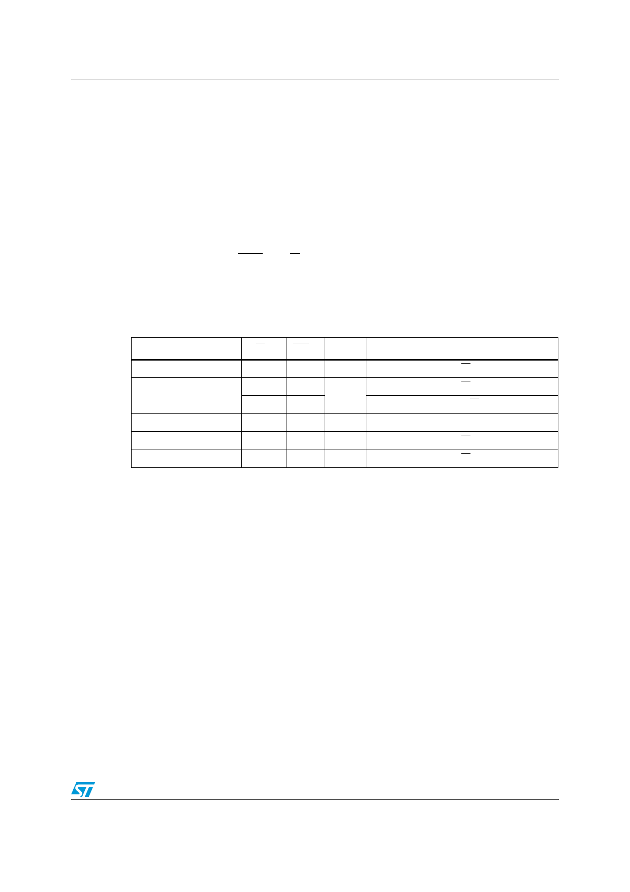
Table 5. Operating modes
Mode
RW bit WC(1) Bytes
Initial sequence
Current Address Read
1
0
Random Address Read
1
Sequential Read
1
Byte Write
0
Page Write
0
1. X = VIH or VIL.
X
1 Start, device select, RW = 1
X
Start, device select, RW = 0, Address
1
X
reStart, device select, RW = 1
X
≥ 1 Similar to Current or Random Address Read
VIL
1 Start, device select, RW = 0
VIL ≤ 256 Start, device select, RW = 0
Doc ID 12943 Rev 7
13/37
Share Link: 