LTC1516 데이터 시트보기 (PDF) - Linear Technology
부품명
상세내역
일치하는 목록
LTC1516 Datasheet PDF : 8 Pages
| |||
LTC1516
APPLICATIONS INFORMATION
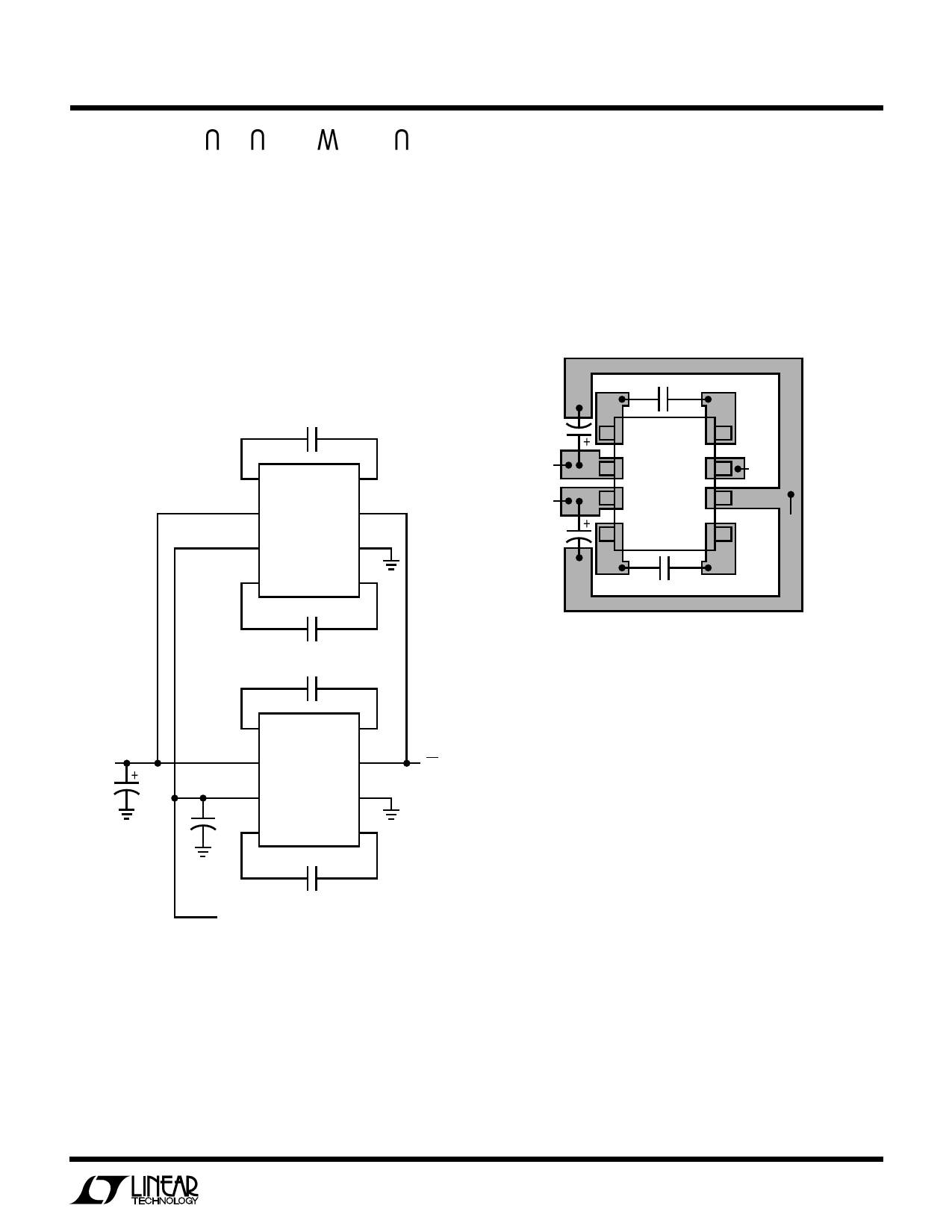
Paralleling Devices
Two or more LTC1516’s may be connected in parallel to
provide higher output currents. The VIN, VOUT, GND and
SHDN pins may be tied together, but the C1 and C2 pins
must be kept separate (see Figure 5). Separate CIN and
COUT capacitors may be required to reduce output noise
and ripple if the paralleled devices cannot be kept close
together. Otherwise, single CIN and COUT capacitors may
be used with each being 2× (or 3× if three parts are
paralleled, etc.) in value.
General Layout Considerations
Due to the high switching frequency and high transient
currents produced by the LTC1516, careful board layout is
a must. A clean board layout using a ground plane and
short connections to all capacitors will improve perfor-
mance and ensure proper regulation under all conditions
(refer to Figure 6).
C1
0.22µF
1 C1+
C1– 8
2 VIN
SHDN 7
LTC1516
3 VOUT
GND 6
4 C2+
C2– 5
0.22µF
CIN
VIN
VOUT
COUT
1
2
LTC1516
3
4
8
7 SHDN
6
GND
5
C2
1516 • F06
0.22µF
Figure 6. Suggested Component Placement for LTC1516
VIN = 2V
TO 5V
22µF
1 C1+
C1– 8
2 VIN
SHDN 7
LTC1516
3 VOUT
GND 6
+
22µF 4 C2+
C2– 5
0.22µF
ON/OFF
VOUT = 5V ±4%
IOUT = 0mA TO 40mA, VIN ≥ 2V
IOUT = 0mA TO 100mA, VIN ≥ 3V
Figure 5. Paralleling Devices
1516 • F05
Information furnished by Linear Technology Corporation is believed to be accurate and reliable.
However, no responsibility is assumed for its use. Linear Technology Corporation makes no represen-
tation that the interconnection of its circuits as described herein will not infringe on existing patent rights.
7
Share Link: 