LTC1516 데이터 시트보기 (PDF) - Linear Technology
부품명
상세내역
일치하는 목록
LTC1516 Datasheet PDF : 8 Pages
| |||
LTC1516
APPLICATIONS INFORMATION
Short-Circuit/Thermal Protection
During short-circuit conditions, the LTC1516 will draw
between 200mA and 400mA from VIN causing a rise in
the junction temperature. On-chip thermal shutdown
circuitry disables the charge pump once the junction
temperature exceeds 135°C, and reenables the charge
pump once the junction temperature falls back to 115°C.
The LTC1516 will cycle in and out of thermal shutdown
indefinitely without latchup or damage until the VOUT short
is removed.
Capacitor Selection
For best performance, it is recommended that low ESR
capacitors be used for both CIN and COUT to reduce noise
and ripple. The CIN and COUT capacitors should be either
ceramic or tantalum and should be 10µF or greater. If the
input source impedance is very low, CIN may not be
needed. Increasing the size of COUT to 22µF or greater will
reduce output voltage ripple.
Ceramic or tantalum capacitors are recommended for the
flying caps C1 and C2 with values in the range of 0.1µF to
1µF. Note that large value flying caps (> 0.22µF) will
increase output ripple unless COUT is also increased. For
very low load applications, C1 and C2 may be reduced to
0.01µF to 0.047µF. This will reduce output ripple at the
expense of efficiency and maximum output current.
Output Ripple
Normal LTC1516 operation produces voltage ripple on the
VOUT pin. Output voltage ripple is required for the LTC1516
to regulate. Low frequency ripple exists due to the hyster-
esis in the sense comparator and propagation delays in the
charge pump enable/disable circuits. High frequency ripple
is also present mainly due to ESR (Equivalent Series
Resistance) in the output capacitor. Typical output ripple
under maximum load is 100mVP-P with a low ESR 10µF
output capacitor.
The magnitude of the ripple voltage depends on several
factors. High input voltages (VIN > 3.3V) increase the output
ripple since more charge is delivered to COUT per clock
cycle. Large C1 and C2 flying capacitors (> 0.22µF) also
increase ripple for the same reason. Large output current
load and/or a small output capacitor (< 10µF) results in
higher ripple due to higher output voltage dV/dt. High ESR
capacitors (ESR > 0.5Ω) on the output pin cause high
frequency voltage spikes on VOUT with every clock cycle.
There are several ways to reduce the output voltage ripple.
A larger COUT capacitor (22µF or greater) will reduce both
the low and high frequency ripple due to the lower COUT
charging and discharging dV/dt and the lower ESR typi-
cally found with higher value (larger case size) capacitors.
A low ESR ceramic output capacitor will minimize the high
frequency ripple, but will not reduce the low frequency
ripple unless a high capacitance value is chosen. A reason-
able compromise is to use a 10µF to 22µF tantalum
capacitor in parallel with a 1µF to 3.3µF ceramic capacitor
on VOUT to reduce both the low and high frequency ripple.
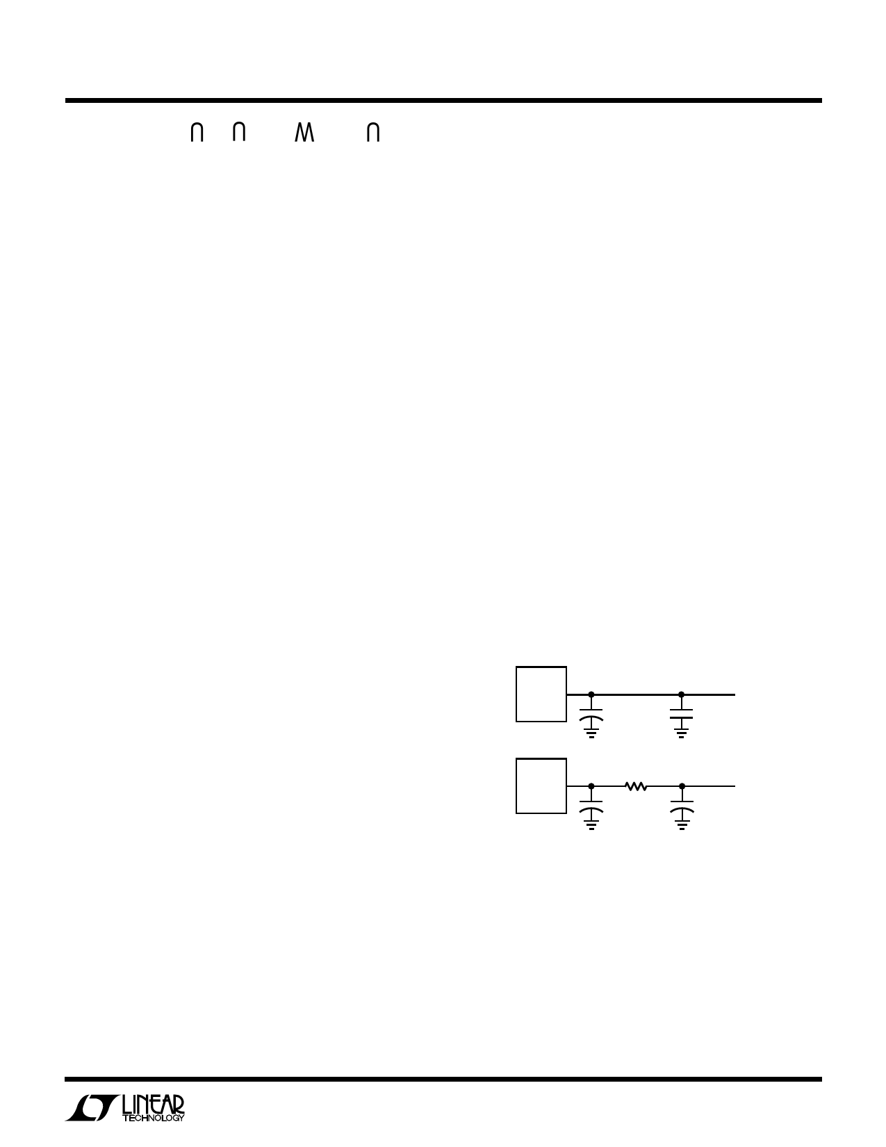
An RC filter may also be used to reduce high frequency
voltage spikes (see Figure 2).
In low load or high VIN applications, smaller values for C1
and C2 may be used to reduce output ripple. The smaller
C1 and C2 flying capacitors (0.022µF to 0.1µF) deliver less
charge per clock cycle to the output capacitor resulting in
lower output ripple. However, the smaller value flying caps
also reduce the maximum IOUT capability as well as
efficiency.
LTC1516
3
VOUT +
15µF
TANTALUM
VOUT
5V
1µF
CERAMIC
LTC1516
3
VOUT +
2Ω
10µF
VOUT
+
5V
10µF
1516 F02
Figure 2. Output Ripple Reduction Techniques
Inrush Currents
During normal operation, VIN will experience current tran-
sients in the 100mA to 200mA range whenever the charge
pump is enabled. During start-up, these inrush currents
may approach 500mA. For this reason, it is important to
minimize the source resistance between the input supply
and the VIN pin to prevent start-up problems and large
input voltage transients.
5
Share Link: 