LC86E6560 데이터 시트보기 (PDF) - SANYO -> Panasonic
부품명
상세내역
일치하는 목록
LC86E6560 Datasheet PDF : 21 Pages
| |||
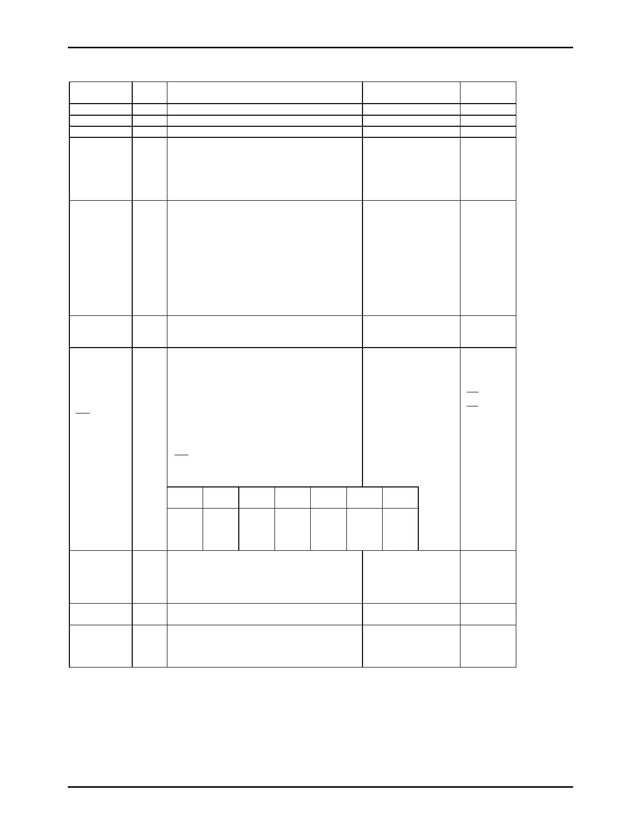
Pin Description
LC86E6560
Pin Name
I/O
Function description
Option
EPROM
mode
VSS1, 2
- Power pin (-)
*4
-
-
VDD1, 2, 3, 4 - Power pin (+)
*4
-
-
VP
- Power pin (+) for the VFD output pull-down resist -
-
PORT 0
P00 - P07
I/O •8-bit input/output port
Input/output in nibble units
•Input for port0 interrupt
•Input for HOLD release
•15V withstand at N-channel open drain output
•Pull-up resistor :
-
Provided/not provided
(each nibble)
•Output form :
CMOS/N-channel
open drain (each bit)
PORT 1
P10 - P17
I/O •8-bit input/output port
Input/output can be specified in bit unit.
•Other pin functions
P10 SIO0 data output
P11 SIO0 data input/bus input/output
P12 SIO0 clock input/output
P13 SIO1 data output
P14 SIO1 data input/bus input/output
P15 SIO1 clock input/output
P16 Buzzer output
P17 Timer1 output (PWM0 output)
Output form :
CMOS/N-channel open
drain (each bit)
Data line
D0 to D7
PORT 3
P30 - P37
I/O •8-bit input/output port
Input/output in bit unit
•15V withstand at N-channel open drain output
Output form :
-
CMOS/N-channel open
drain (each bit)
PORT 7
P70 - P73
P74 - P75
•4-bit input/output port
-
Input/output in bit unit
•2-bit input port
•Other pin functions
I/O P70 : INT0 input/HOLD release/N-channel Tr.
output for watchdog timer
I
P71 : INT1 input/HOLD release input
P72 : INT2 input/timer0 event input
P73 : INT3 input with noise filter/timer0 event
input
EPROM
control
signal
DASEC(*1)
OE (*2)
CE (*3)
P74 : 32.768kHz crystal oscillation terminal XT1
P75 : 32.768kHz crystal oscillation terminal XT2
•Interrupt received form, vector address
rising falling rising/ H level L level Vector
falling
INT0 enable enable disable enable enable 03H
INT1 enable enable disable enable enable 0BH
INT2 enable enable enable disable disable 13H
INT3 enable enable enable disable disable 1BH
PORT 8
•4-bit input/output port
-
-
Input/output in bit unit
P80 -P83
I •4-bit input port
P84 -P87
I/O •Other function
AD input port (8 port pins)
S0/T0 to
O Output for VFD display controller segment/timing -
-
S6/T6 *6
in common
S7/T7 to
O •Output for VFD display controller segment
-
S15/T15
/timing with internal pull-down resistor in
*7
common
•Internal pull-down resistor output
TA (*5)
(Continue)
No.6750-7/21
Share Link: 