LC86E6560 데이터 시트보기 (PDF) - SANYO -> Panasonic
부품명
상세내역
일치하는 목록
LC86E6560 Datasheet PDF : 21 Pages
| |||
LC86E6560
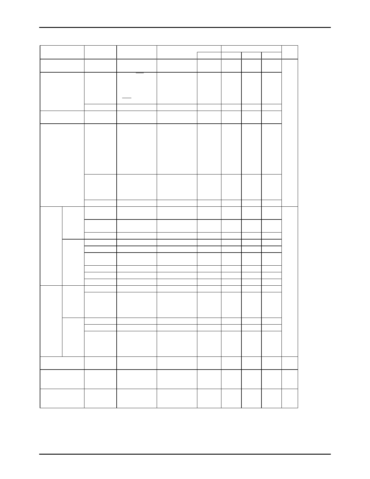
1. Absolute Maximum Ratings at VSS1=VSS2=0V and Ta=25°C
Parameter
Supply voltage
Input voltage
Symbol
VDDMAX
VI(1)
Output voltage
Input/output
voltage
VI(2)
VO
VIO(1)
VIO(2)
High
level
output
current
Peak
output
current
Total
output
current
VIO(3)
IOPH(1)
IOPH(2)
IOPH(3)
∑IOAH(1)
∑IOAH(2)
∑IOAH(3)
Low
level
output
current
Peak
output
current
∑IOAH(4)
∑IOAH(5)
∑IOAH(6)
IOPL(1)
IOPL(2)
Total
output
current
∑IOAL(1)
∑IOAL(2)
∑IOAL(3)
Maximum power
dissipation
Operating
temperature
range
Storage
temperature
range
Pdmax
Topr
Tstg
Pins
VDD1, VDD2
VDD3, VDD4
•Ports P74 , 75
•Ports 80, 81,
82, 83
•Port 8
• RES
VP
S0/T0 to
S15/T15
•Port 1
•Ports 70, 71,
72, 73
•Ports 84, 85,
86, 87
•Ports 0, 3 at
CMOS output
option
Ports 0, 3 at
N-ch open
drain output
option
S16 to S51
Ports 0, 1, 3
S0/T0 to
S15/T15
S16 to S51
Port 0
Ports 1, 3
S0/T0 to
S15/T15
S16 to S27
S28 to S39
S40 to S51
Ports 0, 1, 3
•Ports 70, 71,
72, 73
•Ports 84, 85,
86, 87
Port 0
Ports 1, 3, 70
•Ports 71, 72,
73
•Ports 84, 85,
86, 87
QFC100S
Conditions
Ratings
unit
VDD[V] min. typ. max.
VDD1=VDD2
-0.3
7.0 V
=VDD3=VDD4
-0.3
VDD+0.3
VDD-4.5
VDD-4.5
-0.3
VDD+0.3
VDD+0.3
VDD+0.3
•CMOS output
•For each pin.
At each pin.
At each pin.
The total all pins.
The total all pins.
The total all pins.
The total all pins.
The total all pins.
The total all pins.
At each pin.
At each pin.
The total all pins.
The total all pins.
The total all pins.
Ta=+10 to +40°C
-0.3
15
VDD-4.5
-10
-30
-15
-30
-30
-55
-60
-60
-60
VDD+0.3
mA
20
15
60
50
20
500 mW
+10
+40 °C
-55
+125 °C
No.6750-10/21
Share Link: 