L3G4200D 데이터 시트보기 (PDF) - STMicroelectronics
부품명
상세내역
일치하는 목록
L3G4200D Datasheet PDF : 24 Pages
| |||
L3G4200D
Digital interfaces
5.2.1
SPI read
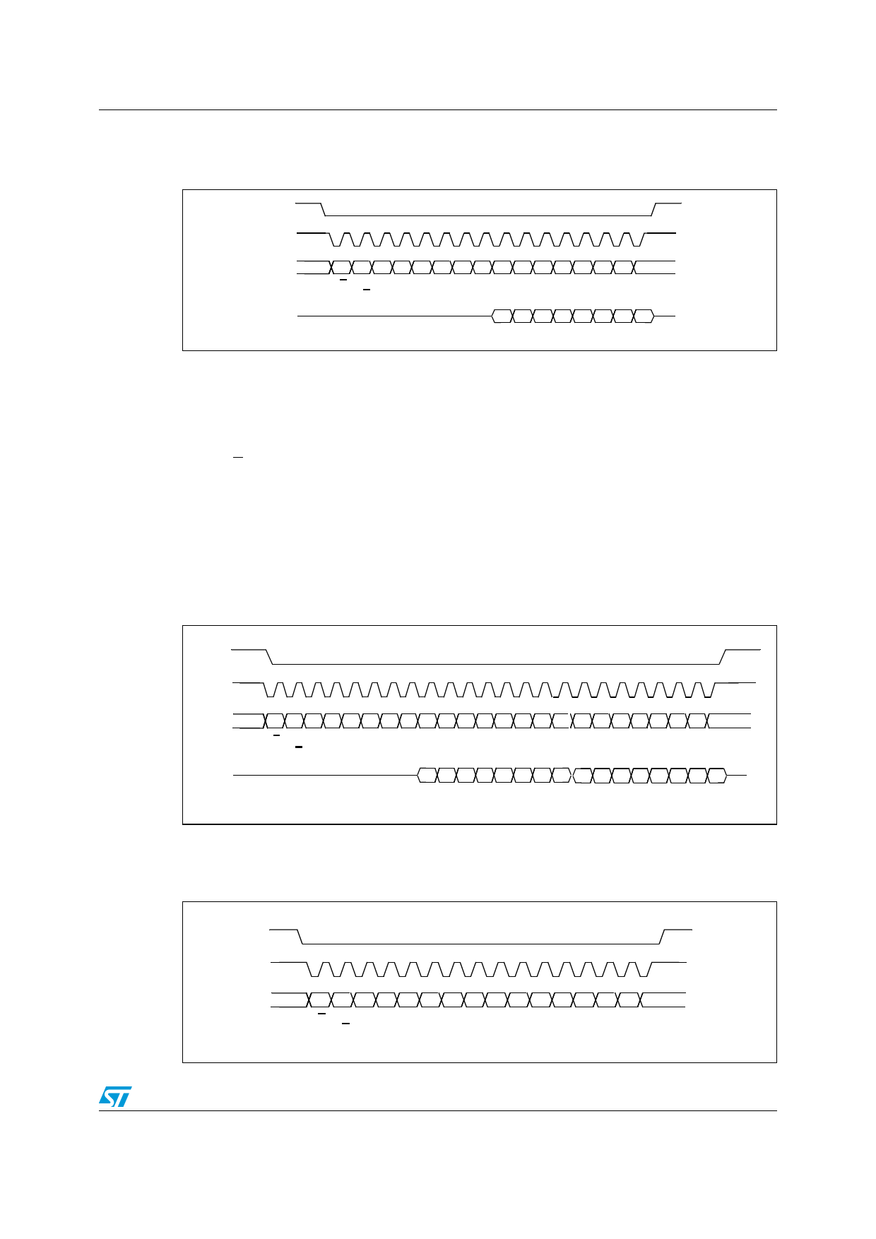
Figure 8. SPI read protocol
CS
SPC
SDI
SDO
RW
MS AD5 AD4 AD3 AD2 AD1 AD0
DO7 DO6 DO5 DO4 DO3 DO2 DO1 DO0
The SPI Read command is performed with 16 clock pulses. Multiple byte read command is
performed adding blocks of 8 clock pulses at the previous one.
bit 0: READ bit. The value is 1.
bit 1: MS bit. When 0 do not increment address, when 1 increment address in multiple
reading.
bit 2-7: address AD(5:0). This is the address field of the indexed register.
bit 8-15: data DO(7:0) (read mode). This is the data that will be read from the device (MSb
first).
bit 16-... : data DO(...-8). Further data in multiple byte reading.
Figure 9. Multiple bytes SPI read protocol (2 bytes example)
CS
SPC
SDI
SDO
RW
MS AD5 AD4 AD3 AD2 AD1 AD0
DO7 DO6 DO5 DO4 DO3 DO2 DO1 DO0 DO15DO14DO13DO12DO11DO10DO9 DO8
5.2.2
SPI write
Figure 10. SPI write protocol
CS
SPC
SDI
RW
DI7 DI6 DI5 DI4 DI3 DI2 DI1 DI0
MS AD5 AD4 AD3 AD2 AD1 AD0
Doc ID 17116 Rev 1
19/24
Share Link: 