K4S560432B-TC/L75 데이터 시트보기 (PDF) - Samsung
부품명
상세내역
일치하는 목록
K4S560432B-TC/L75 Datasheet PDF : 11 Pages
| |||
K4S560432B
CMOS SDRAM
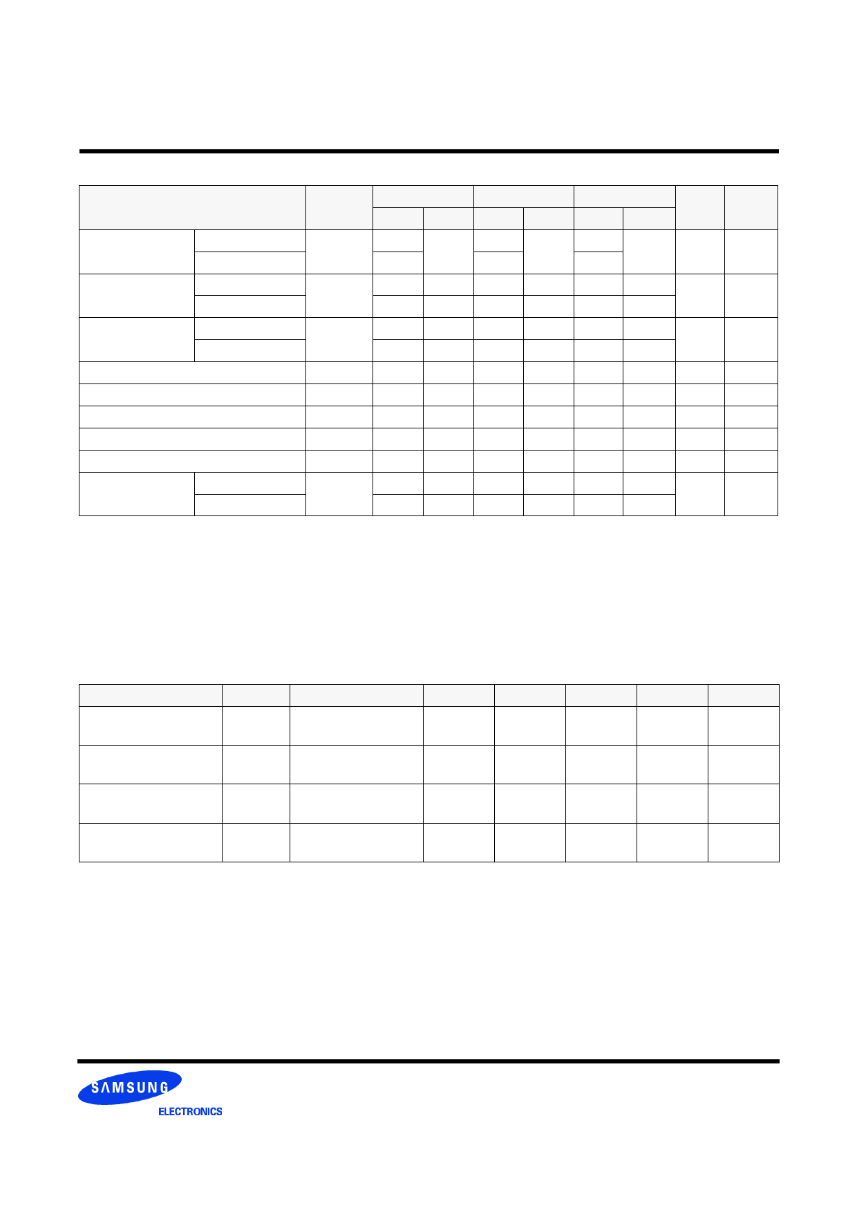
AC CHARACTERISTICS (AC operating conditions unless otherwise noted)
Parameter
CLK cycle time
CAS latency=3
CAS latency=2
CLK to valid
output delay
CAS latency=3
CAS latency=2
Output data
hold time
CAS latency=3
CAS latency=2
CLK high pulse width
CLK low pulse width
Input setup time
Input hold time
CLK to output in Low-Z
CLK to output
in Hi-Z
CAS latency=3
CAS latency=2
Symbol
tCC
tSAC
tOH
tCH
tCL
tSS
tSH
tSLZ
tSHZ
-75
Min Max
7.5
1000
-
5.4
-
3
-
2.5
2.5
1.5
0.8
1
5.4
-
-1H
-1L
Unit Note
Min Max Min Max
10
10
1000
1000
ns
1
10
12
6
6
ns
1, 2
6
7
3
3
ns
2
3
3
3
3
ns
3
3
3
ns
3
2
2
ns
3
1
1
ns
3
1
1
ns
2
6
6
ns
6
7
Notes : 1. Parameters depend on programmed CAS latency.
2. If clock rising time is longer than 1ns, (tr/2-0.5)ns should be added to the parameter.
3. Assumed input rise and fall time (tr & tf) = 1ns.
If tr & tf is longer than 1ns, transient time compensation should be considered,
i.e., [(tr + tf)/2-1]ns should be added to the parameter.
DQ BUFFER OUTPUT DRIVE CHARACTERISTICS
Parameter
Symbol
Condition
Min
Typ
Max
Output rise time
trh
Measure in linear
region : 1.2V ~ 1.8V
1.37
4.37
Output fall time
tfh
Measure in linear
region : 1.2V ~ 1.8V
1.30
3.8
Output rise time
trh
Measure in linear
region : 1.2V ~ 1.8V
2.8
3.9
5.6
Output fall time
tfh
Measure in linear
region : 1.2V ~ 1.8V
2.0
2.9
5.0
Notes : 1. Rise time specification based on 0pF + 50 Ω to VSS, use these values to design to.
2. Fall time specification based on 0pF + 50 Ω to VDD, use these values to design to.
3. Measured into 50pF only, use these values to characterize to.
4. All measurements done with respect to VSS.
Unit
Volts/ns
Volts/ns
Volts/ns
Volts/ns
Notes
3
3
1,2
1,2
Rev. 0.2 May.2000
Share Link: 