C3225X7R1E106M 데이터 시트보기 (PDF) - Intersil
부품명
상세내역
일치하는 목록
C3225X7R1E106M Datasheet PDF : 20 Pages
| |||

ISL97650B
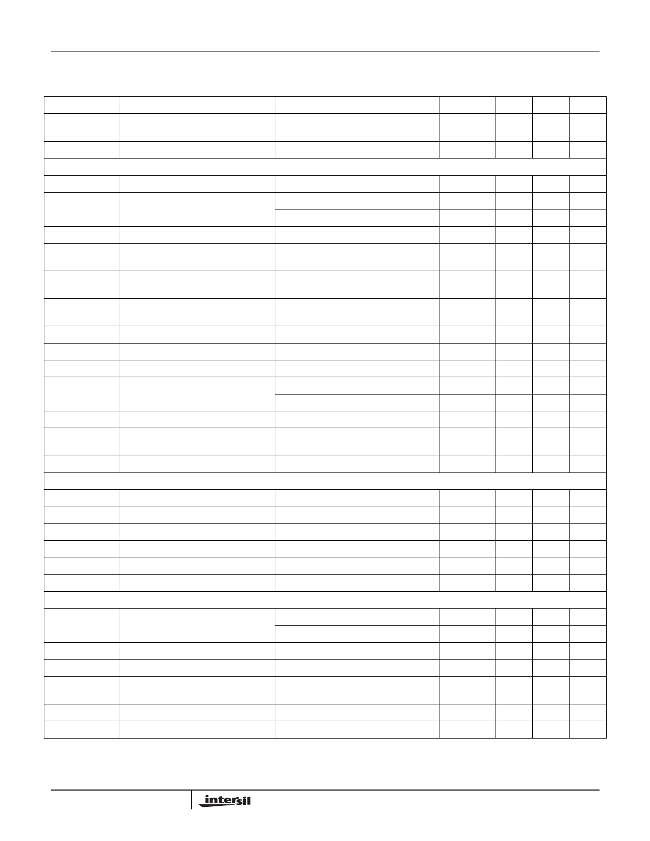
Electrical Specifications
VIN = 12V, VBOOST = VSUP = 15V, VON = 25V, VOFF = -8V, over temperature from -40°C to +105°C; Parameters
with MIN and/or MAX limits are 100% tested at +25°C, unless otherwise specified. Temperature limits established
by characterization and are not production tested. (Continued)
PARAMETER
DESCRIPTION
CONDITIONS
MIN
TYP MAX UNIT
D_NCP_max
Max Duty Cycle of the Negative Charge
Pump
50
%
Rpd(FBN)off
Pull-Down Resistance, Not Active
I(FBN) = 500µA
1.5
3.3
5.5
kΩ
POSITIVE (VON) CHARGE PUMP
VON
VON Output Voltage Range
ILoad_PCP_min External Load Driving Capability
RON(VSUP_SW) ON-Resistance of VSUP Input Switch
RON(C1/2-)H
High-Side Driver ON-Resistance at
C1- and C2-
2x or 3x Charge Pump
VON = 25V (2x Charge Pump)
VON = 34V (3x Charge Pump)
I(switch) = +40mA
I(C1/2-) = +40mA
VSUP +2V
20
20
10
34
V
mA
mA
17
Ω
30
Ω
RON(C1/2-)L
Low-Side Driver ON-Resistance at
C1- and C2-
I(C1/2-) = -40mA
4
7
Ω
Ipu(VSUP_SW) Pull-Up Current Limit in VSUP Input
V(C2+) = 0V to V(SUP) - 0.4V - V(diode)
40
100
mA
Switch
Ipu(C1/2-)
Pull-Up Current Limit in C1- and C2- V(C1/2-) = 0V to V(VSUP) - 0.4V
40
100
mA
Ipd(C1/2-)
Pull-Down Current Limit in C1- and C2- V(C1/2-) = 0.2V to V(VSUP)
-100
-40
mA
I(POUT)leak
VFBP
Leakage Current in POUT
FBP Regulation Voltage
EN = LOW
TA = +25°C
-5
1.176
1.172
5
µA
1.2 1.224
V
1.2 1.228
V
ACCP
D_PCP_max
VON Output Accuracy
Max Duty Cycle of the Positive Charge
Pump
ION = 1mA, TA = +25°C
-2
+2
%
50
%
V(diode)
Internal Schottky Diode Forward Voltage I(diode) = +40mA
700
800
mV
ENABLE INPUTS
VHI-EN
Enable “HIGH”
2.2
V
VLO_EN
Enable “LOW”
0.8
V
IEN_pd
VHI-ENL
Enable Pin Pull-Down Current
Logic Enable “HIGH”
VEN > VLO_EN
25
µA
2.2
V
VLO-ENL
Logic Enable “LOW”
0.8
V
IENL_pd
Logic Enable Pin Pull-Down Current
VON SLICE POSITIVE SUPPLY = V(POUT)
I(POUT)_slice
VON Slice Current from POUT Supply
VENL > VLO_ENL
CTL = VDD, sequence complete
CTL = AGND, sequence complete
25
µA
200
400
µA
100
150
µA
RON(POUT-COM) ON-Resistance between POUT - COM CTL = VDD, sequence complete
RON(DRN-COM) ON-Resistance between DRN - COM CTL = ACGND, sequence complete
5
10
Ω
30
60
Ω
RON_COM
ON-Resistance between COM and
PGND3
200
500 1500
Ω
VLO
CTL Input LOW Voltage
0.8
V
VHI
CTL Input HIGH Voltage
2.2
V
4
FN6748.1
March 22, 2010