ISL97650 데이터 시트보기 (PDF) - Intersil
부품명
상세내역
일치하는 목록
ISL97650 Datasheet PDF : 20 Pages
| |||
ISL97650
Absolute Maximum Ratings (TA = +25°C)
Maximum Pin Voltages, all pins except below . . . . . . . . . . . . . . 6.5V
LX1, LX2, VSUP, NOUT, DELB, C2- . . . . . . . . . . . . . . . . . . . .24V
C1- . . . . . . . . . . . . . . . . . . . . . . . . . . . . . . . . . . . . . . . . . . . . . .14V
VIN1, VINL . . . . . . . . . . . . . . . . . . . . . . . . . . . . . . . . . . . . . . 16.5V
DRN, COM, POUT, C1+, C2+ . . . . . . . . . . . . . . . . . . . . . . . . .36V
CB . . . . . . . . . . . . . . . . . . . . . . . . . . . . . . . . . . . . . . . . . . . . . .21V
Recommended Operating Conditions
Input Voltage Range, VIN . . . . . . . . . . . . . . . . . . . . . . . . 4V to 14V
Boost Output Voltage Range, AVDD . . . . . . . . . . . . . . . . . . . . +20V
VON Output Range, VON . . . . . . . . . . . . . . . . . . . . . . +15V to +32V
VOFF Output Range, VOFF . . . . . . . . . . . . . . . . . . . . . . . -15V to -5V
Logic Output Voltage Range, VLOGIC . . . . . . . . . . . . +1.5V to +3.3V
Input Capacitance, CIN . . . . . . . . . . . . . . . . . . . . . . . . . . . . . 2x10µF
Boost Inductor, L1 . . . . . . . . . . . . . . . . . . . . . . . . . . . . . 3.3µH-10µH
Output Capacitance, COUT . . . . . . . . . . . . . . . . . . . . . . . . . . 2x22µF
Buck Inductor, L2 . . . . . . . . . . . . . . . . . . . . . . . . . . . . .3.3µH to10µH
Operating Ambient Temperature Range . . . . . . . . -40°C to +105°C
Operating Junction Temperature . . . . . . . . . . . . . . -40°C to +125°C
Thermal Information
Thermal Resistance
θJA (°C/W) θJC (°C/W)
6x6 QFN Package (Notes 1, 2) . . . . . .
30
2.5
Maximum Junction Temperature (Plastic Package) . . . . . . . +150°C
Maximum Storage Temperature Range . . . . . . . . . .-65°C to +150°C
Power Dissipation
TA ≤ +25°C . . . . . . . . . . . . . . . . . . . . . . . . . . . . . . . . . . . . . . .3.3W
TA = +70°C. . . . . . . . . . . . . . . . . . . . . . . . . . . . . . . . . . . . . . .1.8W
TA = +85°C. . . . . . . . . . . . . . . . . . . . . . . . . . . . . . . . . . . . . . .1.3W
TA = +100°C. . . . . . . . . . . . . . . . . . . . . . . . . . . . . . . . . . . . . .0.8W
Pb-Free Reflow Profile. . . . . . . . . . . . . . . . . . . . . . . . .see link below
http://www.intersil.com/pbfree/Pb-FreeReflow.asp
CAUTION: Do not operate at or near the maximum ratings listed for extended periods of time. Exposure to such conditions may adversely impact product reliability and
result in failures not covered by warranty.
NOTES:
1. θJA is measured in free air with the component mounted on a high effective thermal conductivity test board with “direct attach” features. See
Tech Brief TB379.
2. For θJC, the “case temp” location is the center of the exposed metal pad on the package underside.
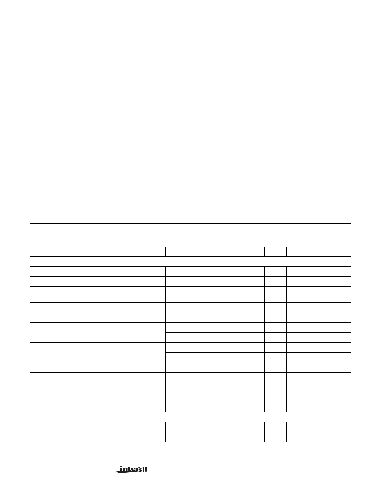
Electrical Specifications
VIN = 12V, VBOOST = VSUP = 15V, VON = 25V, VOFF = -8V, over-temperature from -40°C to +105°C, unless
otherwise stated. Parameters with MIN and/or MAX limits are 100% tested at +25°C, unless otherwise
specified. Temperature limits established by characterization and are not production tested.
PARAMETER
DESCRIPTION
CONDITIONS
MIN TYP MAX UNIT
SUPPLY PINS
VIN
VINL
VSUP
Supply Voltage (VIN1)
Logic Supply Voltage
Charge Pumps and VON Slice Positive
Supply
4
12
14
V
4
12
14
V
4
20
V
IVIN
Quiescent Current into VIN
Enabled, No switching
Disabled
3
5
mA
25
50
µA
IINL
Logic Supply Current
Enabled, No switching
Disabled
0.25
2
mA
1
25
µA
ISUP
VSUP Supply Current
Enabled, No Switching and VPout = VSUP
Disabled
1
mA
1
10
µA
VLOR
VLOF
VREF
Undervoltage Lockout Threshold
Undervoltage Lockout Threshold
Reference Voltage
VDC rising
VDC falling
TA = +25°C
3.85
4
V
3.3
3.45
V
1.18 1.205 1.225
V
1.177 1.205 1.228
V
FOSC
AVDD BOOST
DMIN
DMAX
Oscillator Frequency
Minimum Duty Cycle
Maximum Duty Cycle
1020 1200 1380 kHz
20
25
%
84
%
2
FN9198.4
April 17, 2009
Share Link: 