IRF320 데이터 시트보기 (PDF) - Intersil
부품명
상세내역
일치하는 목록
IRF320 Datasheet PDF : 7 Pages
| |||
IRF320, IRF321, IRF322, IRF323
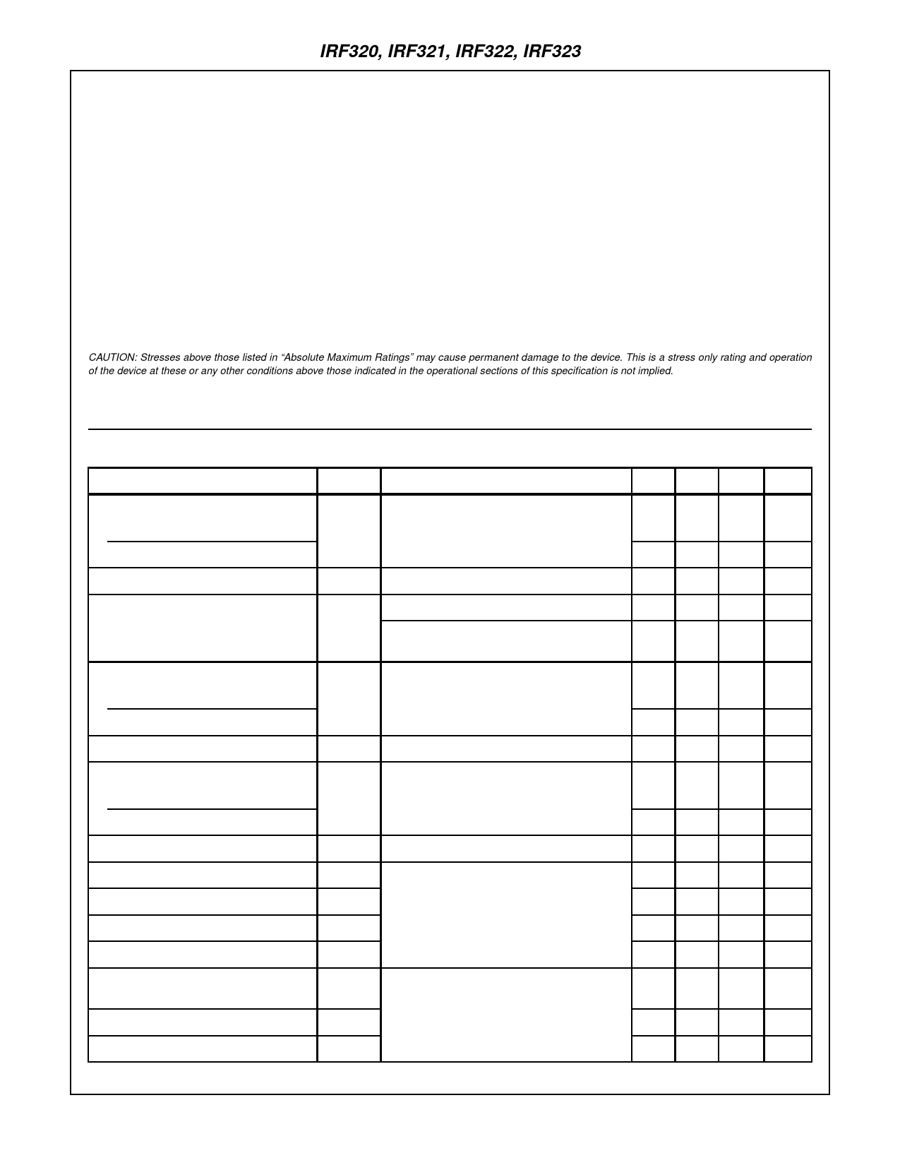
Absolute Maximum Ratings TC = 25oC, Unless Otherwise Specified
IRF320
Drain to Source Breakdown Voltage (Note 1). . . . . . . . . .VDS
400
Drain to Gate Voltage (RGS = 20kΩ) (Note 1) . . . . . . . VDGR
400
Continuous Drain Current. . .
TC = 100oC . . . . . . . . . . . .
...........
...........
...
...
.........
.........
ID
ID
3.3
2.1
Pulsed Drain Current (Note 3) . . . . . . . . . . . . . . . . . . . . . IDM
13
Gate to Source Voltage . . . . . . . . . . . . . . . . . . . . . . . . . .VGS
±20
Maximum Power Dissipation . . . . . . . . . . . . . . . . . . . . . . . PD
50
Linear Derating Factor . . . . . . . . . . . . . . . . . . . . . . . . . . . .
0.4
Single Pulse Avalanche Energy Rating (Note 4) . . . . . . . EAS
Operating and Storage Temperature . . . . . . . . . . . . TJ, TSTG
Maximum Temperature for Soldering
Leads at 0.063in (1.6mm) from Case for 10s . . . . . . . . . TL
Package Body for 10s, See TB334 . . . . . . . . . . . . . . . Tpkg
190
-55 to 150
300
260
IRF321
350
350
3.3
2.1
13
±20
50
0.4
190
-55 to 150
300
260
IRF322
400
400
2.8
1.8
11
±20
50
0.4
190
-55 to 150
300
260
IRF323
350
350
2.8
1.8
11
±20
50
0.4
190
-55 to 150
300
260
UNITS
V
V
A
A
A
V
W
W/oC
mJ
oC
oC
oC
CAUTION: Stresses above those listed in “Absolute Maximum Ratings” may cause permanent damage to the device. This is a stress only rating and operation
of the device at these or any other conditions above those indicated in the operational sections of this specification is not implied.
NOTE:
1. TJ = 25oC to 125oC.
Electrical Specifications TC = 25oC, Unless Otherwise Specified
PARAMETER
SYMBOL
TEST CONDITIONS
MIN TYP MAX UNITS
Drain to Source Breakdown Voltage
IRF320, IRF322
BVDSS ID = 250µA, VGS = 0V, (Figure 10)
400
-
-
V
IRF321, IRF323
350
-
-
V
Gate to Threshold Voltage
Zero Gate Voltage Drain Current
On-State Drain Current (Note 2)
IRF320, IRF321
VGS(TH) VGS = VDS, ID = 250µA
IDSS VDS = Rated BVDSS, VGS = 0V
VDS = 0.8 x Rated BVDSS, VGS = 0V
TJ = 125oC
ID(ON) VDS > ID(ON) x rDS(ON)MAX, VGS = 10V
(Figure 7)
2.0
-
4.0
V
-
-
25
µA
-
-
250
µA
3.3
-
-
A
IRF322, IRF323
2.8
-
-
A
Gate to Source Leakage Current
Drain to Source On Resistance (Note 2)
IRF320, IRF321
IGSS VGS = ±20V
rDS(ON) ID = 1.8A, VGS = 10V, (Figures 8, 9)
±100 nA
-
1.5 1.8
Ω
IRF322, IRF323
-
1.8 2.5
Ω
Forward Transconductance (Note 2)
Turn-On Delay Time
Rise Time
Turn-Off Delay Time
Fall Time
Total Gate Charge
(Gate to Source + Gate to Drain)
Gate to Source Charge
Gate to Drain “Miller” Charge
gfs
VDS ≥ 10V, ID = 2.0A, (Figure 12)
1.7 2.7
-
S
td(ON) VDD = 200V, ID ≈ 3.3A, RG = 18Ω, RL = 60Ω,
-
10
15
ns
VGS = 10V, (Figures 17, 18)
tr
MOSFET Switching Times are Essentially
-
14
20
ns
Independent of Operating Temperature
td(OFF)
-
30
45
ns
tf
-
13
20
ns
Qg(TOT) VGS = 10V, ID = 3.3A, VDS = 0.8 x Rated BVDSS, -
12
20
nC
IG(REF) = 1.5mA, (Figures 14, 19, 20)
Gate Charge is Essentially Independent of
Qgs Operating Temperature
-
4
-
nC
Qgd
-
8
-
nC
5-2
Share Link: 