IDT72V845 데이터 시트보기 (PDF) - Integrated Device Technology
부품명
상세내역
일치하는 목록
IDT72V845
IDT72V845 Datasheet PDF : 26 Pages
| |||

IDT72V805/72V815/72V825/72V835/72V845
3.3 V CMOS DUAL SyncFIFO™ 256 x 18, 512 x 18, 1,024 x 18, 4,096 x 18
COMMERCIAL AND INDUSTRIAL
TEMPERATURE RANGES
SIGNAL DESCRIPTIONS
INPUTS:
DATA IN (D0 - D17)
Data inputs for 18-bit wide data.
CONTROLS:
RESET (RSA/RSB)
Reset is accomplished whenever the Reset (RSA/RSB) input is taken to
a LOW state. During reset, both internal read and write pointers are set to
the first location. A reset is required after power-up before a write operation
can take place. The Half-Full flag (HFA/HFB) and Programmable Almost-
Full flag (PAFA/PAFB) will be reset to HIGH after tRSF. The Programmable
Almost-Empty flag (PAEA/PAEB) will be reset to LOW after tRSF. The Full
Flag (FFA/FFB) will reset to HIGH. The Empty Flag (EFA/EFB) will reset
to LOW in IDT Standard mode but will reset to HIGH in FWFT mode. During
reset, the output register is initialized to all zeros and the offset registers
are initialized to their default values.
In the IDT Standard mode, every word accessed at Qn, including the first
word written to an empty FIFO, must be requested using REN. When the
last word has been read from the FIFO, the Empty Flag (EFA/EFB) will go
LOW, inhibiting further read operations. REN is ignored when the FIFO is
empty. Once a write is performed, EF will go HIGH allowing a read to occur.
The EF flag is updated on the rising edge of RCLK.
In the FWFT mode, the first word written to an empty FIFO automatically
goes to the outputs Qn, on the third valid LOW to HIGH transition of RCLK
+ tSKEW after the first write. REN does not need to be asserted LOW. In
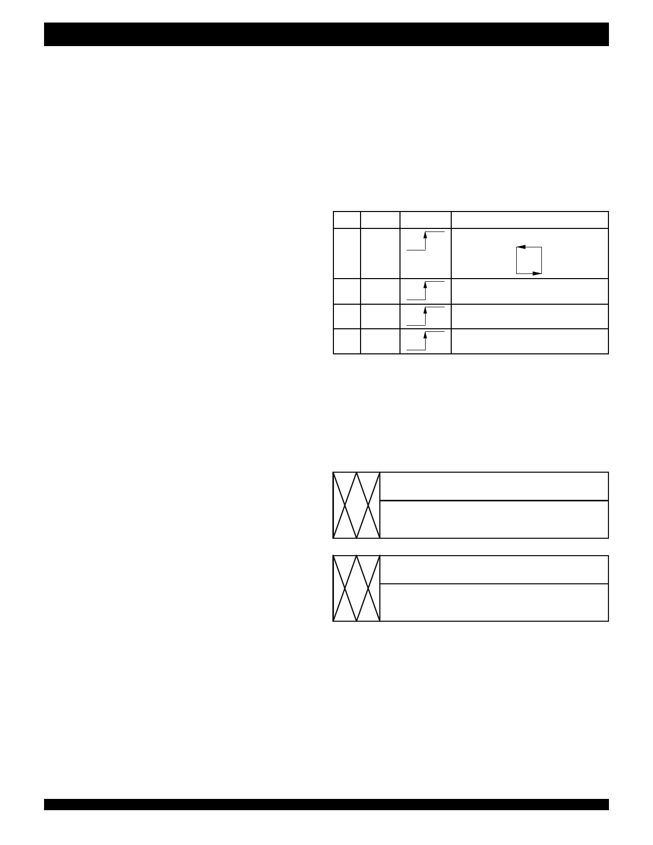
LD WEN
0
0
0
1
WCLK
Selection
Writing to offset registers:
Empty Offset
Full Offset
No Operation
WRITE CLOCK (WCLKA/WCLKB)
A write cycle is initiated on the LOW-to-HIGH transition of the Write
Clock (WCLKA/WCLKB). Data setup and hold times must be met with
respect to the LOW-to-HIGH transition of WCLK.
The Write and Read Clocks can be asynchronous or coincident.
WRITE ENABLE (WENA/WENB)
When the WENA/WENB input is LOW, data may be loaded into the
FIFO RAM array on the rising edge of every WCLK cycle if the device is not
full. Data is stored in the RAM array sequentially and independently of any
ongoing read operation.
When WEN is HIGH, no new data is written in the RAM array on each
WCLK cycle.
To prevent data overflow in the IDT Standard Mode, FF will go LOW,
inhibiting further write operations. Upon the completion of a valid read
cycle, FF will go HIGH allowing a write to occur. The FF flag is updated on
the rising edge of WCLK.
To prevent data overflow in the FWFT mode, Input Ready (IRA,IRB) will
go HIGH, inhibiting further write operations. Upon the completion of a valid
read cycle, IR will go LOW allowing a write to occur. The IR flag is updated
on the rising edge of WCLK.
WEN is ignored when the FIFO is full in either FWFT or IDT Standard
mode.
READ CLOCK (RCLKA/RCLKB)
Data can be read on the outputs on the LOW-to-HIGH transition of the
Read Clock (RCLKA/RCLKB), when Output Enable (OEA/OEB) is set
LOW.
The Write and Read Clocks can be asynchronous or coincident.
1
0
Write Into FIFO
1
1
No Operation
NOTE:
1. The same selection sequence applies to reading from the registers. REN is enabled and
read is performed on the LOW-to-HIGH transition of RCLK.
Figure 2. Writing to Offset Registers
17
11
0
EMPTY OFFSET REGISTER
DEFAULT VALUE
001FH (IDT72V805) 003FH (IDT72V815):
007FH (IDT72V825/72V835/72V845)
17
11
0
FULL OFFSET REGISTER
DEFAULT VALUE
001FH (IDT72V805) 003FH (IDT72V815):
007FH (IDT72V825/72V835/72V845)
NOTE:
4295 drw 04
1. Any bits of the offset register not being programmed should be set to zero.
Figure 3. Offset Register Location and Default Values
READ ENABLE (RENA/RENB)
When Read Enable (RENA/RENB) is LOW, data is loaded from the RAM
array into the output register on the rising edge of every RCLK cycle if the
device is not empty.
When the REN input is HIGH, the output register holds the previous data
and no new data is loaded into the output register. The data outputs Q0-
Qn maintain the previous data value.
order to access all other words, a read must be executed using REN. The
RCLK LOW to HIGH transition after the last word has been read from the
FIFO, Output Ready (ORA/ORB) will go HIGH with a true read (RCLK with
REN = LOW), inhibiting further read operations. REN is ignored when the
FIFO is empty.
9