IDT72205LB 데이터 시트보기 (PDF) - Integrated Device Technology
부품명
상세내역
일치하는 목록
IDT72205LB
Integrated Device Technology

IDT72205LB Datasheet PDF : 21 Pages
| |||
Integrated Device Technology, Inc.
CMOS SyncFIFO™
256 x 18, 512 x 18, 1024 x 18, 2048 x
18 and 4096 x 18
IDT72205LB
IDT72215LB
IDT72225LB
IDT72235LB
IDT72245LB
FEATURES:
• 256 x 18-bit organization array (72205LB)
• 512 x 18-bit organization array (72215LB)
• 1024 x 18-bit organization array (72225LB)
• 2048 x 18-bit organization array (72235LB)
• 4096 x 18-bit organization array (72245LB)
• 15 ns read/write cycle time
• Easily expandable in depth and width
• Read and write clocks can be asynchronous or coincident
• Dual-Port zero fall-through time architecture
• Programmable almost-empty and almost-full flags
• Empty and Full flags signal FIFO status
• Half-Full flag capability in a single device configuration
• Output enable puts output data bus in high-impedance
state
• High-performance submicron CMOS technology
• Available in a 64-lead thin quad flatpack (TQFP/STQFP),
pin grid array (PGA), and plastic leaded chip carrier
(PLCC)
• Military product compliant to MIL-STD-883, Class B
• Industrial temperature range (-40OC to +85OC) is avail-
able, tested to military electrical specifications
DESCRIPTION:
The IDT72205LB/72215LB/72225LB/72235LB/72245LB
are very high-speed, low-power First-In, First-Out (FIFO)
memories with clocked read and write controls. These FIFOs
are applicable for a wide variety of data buffering needs, such
as optical disk controllers, Local Area Networks (LANs), and
interprocessor communication.
Both FIFOs have 18-bit input and output ports. The input
port is controlled by a free-running clock (WCLK), and a data
input enable pin (WEN). Data is read into the synchronous
FIFO on every clock when WEN is asserted. The output port
is controlled by another clock pin (RCLK) and another enable
pin (REN). The read clock can be tied to the write clock for
single clock operation or the two clocks can run asynchronous
of one another for dual-clock operation. An Output Enable pin
(OE) is provided on the read port for three-state control of the
output.
The synchronous FIFOs have two fixed flags, Empty (EF)
and Full (FF), and two programmable flags, Almost-Empty
(PAE) and Almost-Full (PAF). The offset loading of the pro-
grammable flags is controlled by a simple state machine, and
is initiated by asserting the Load pin (LD). A Half-Full flag (HF)
is available when the FIFO is used in a single device configu-
ration.
The IDT72205LB/72215LB/72225LB/72235LB/72245LB
are depth expandable using a daisy-chain technique. The XI
and XO pins are used to expand the FIFOs. In depth expan-
sion configuration, FL is grounded on the first device and set
to HIGH for all other devices in the daisy chain.
The IDT72205LB/72215LB/72225LB/72235LB/72245LB is
fabricated using IDT’s high-speed submicron CMOS technol-
ogy. Military grade product is manufactured in compliance
with the latest revision of MIL-STD-883, Class B.
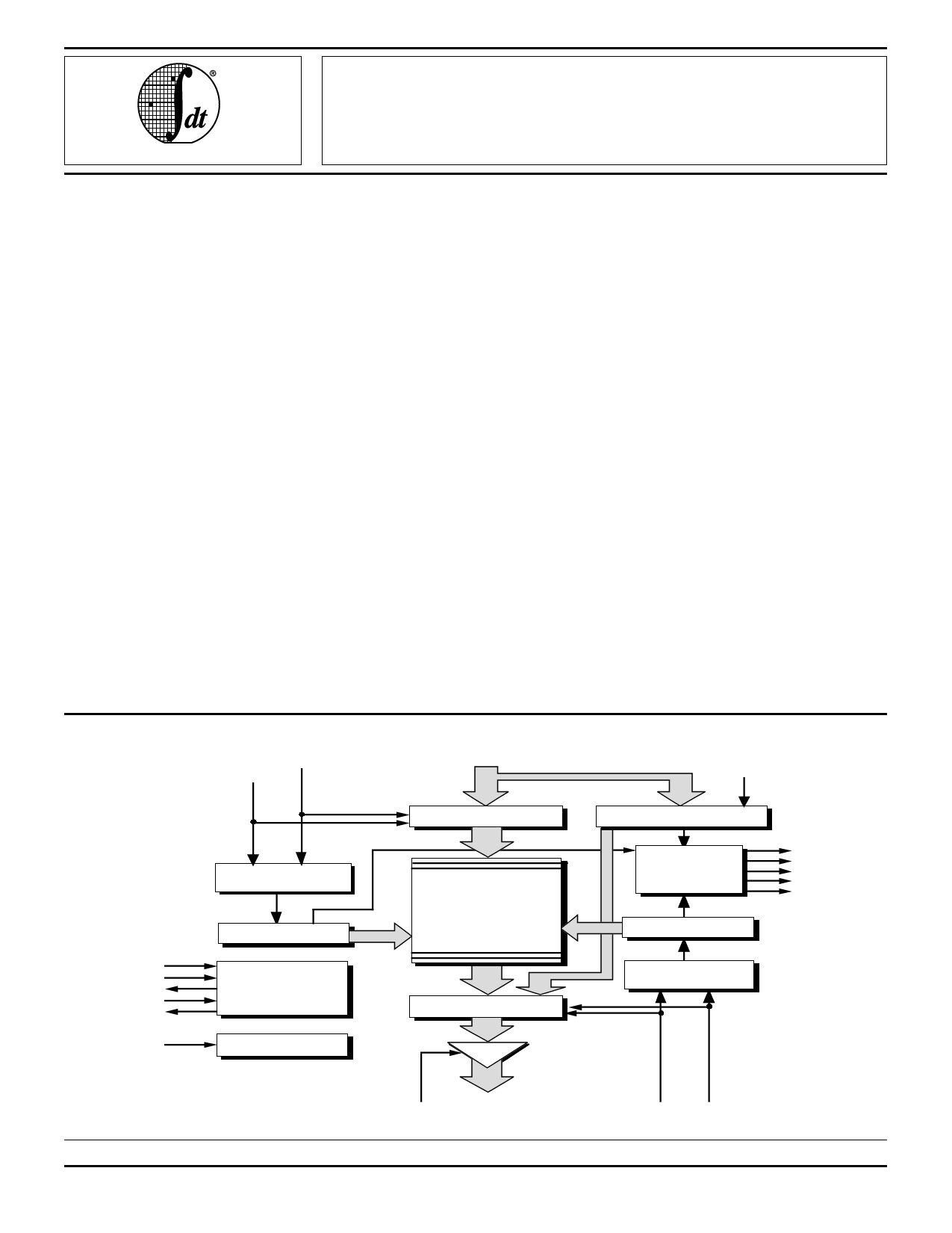
FUNCTIONAL BLOCK DIAGRAM
WCLK
WEN
D0-D17
LD
FL
(HF)/WWRXXXOII
RXO
RS
WRITE CONTROL
LOGIC
WRITE POINTER
EXPANSION LOGIC
RESET LOGIC
INPUT REGISTER
••
RAM ARRAY
256 x 18, 512 x 18
1024 x 18, 2048 x 18
4096 x 18
••
OUTPUT REGISTER
OFFSET REGISTER
FLAG
LOGIC
READ POINTER
READ CONTROL
LOGIC
PHFPEFAFAF/EF(WXO)
OE Q0-Q17
SyncFIFO is a trademark and the IDT logo is a registered trademark of Integrated Device Technology, Inc
RCLK
MILITARY AND COMMERCIAL TEMPERATURE RANGES
©1996 Integrated Device Technology, Inc.
For latest information contact IDT's web site at www.idt.com or fax-on-demand at 408-492-8391.
5.16
REN
2766 drw 01
DECEMBER 1996
DSC-2766/7
1
Share Link: