IDT71321 데이터 시트보기 (PDF) - Integrated Device Technology
부품명
상세내역
일치하는 목록
IDT71321 Datasheet PDF : 13 Pages
| |||
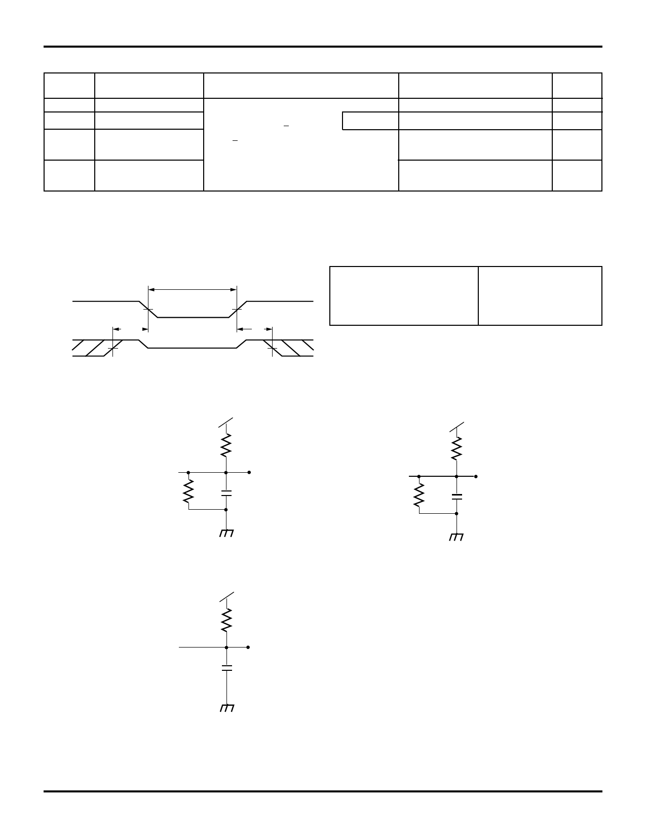
IDT71321SA/LA AND IDT71421SA/LA
HIGH-SPEED 2K x 8 DUAL-PORT STATIC RAM WITH INTERRUPTS
DATA RETENTION CHARACTERISTICS (LA Version Only)
Symbol
Parameter
Test Conditions
VDR
VCC for Data Retention
ICCDR
tCDR(3)
Data Retention Current
Chip Deselect to Data
VCC = 2.0V, CE > VCC - 0.2V COM'L.
VIN > VCC - 0.2V or VIN≤ 0.2V
Retention Time
tR(3)
Operation Recovery
Time
NOTES:
1. VCC = 2V, TA = +25°C, and is not production tested.
2. tRC = Read Cycle Time
3. This parameter is guaranteed by device characterization but not production tested.
COMMERCIAL TEMPERATURE RANGE
71321LA/71421LA
Min.
Typ.(1) Max.
2.0
—
0
—
100
1500
0
—
—
tRC(2)
—
—
Unit
V
µA
ns
ns
2691 tbl 07
DATA RETENTION WAVEFORM
DATA RETENTION MODE
VCC
CE
4.5V
tCDR
VIH
VDR ≥ 2.0V
VDR
4.5V
tR
VIH
AC TEST CONDITIONS
Input Pulse Levels
Input Rise/Fall Times
Input Timing Reference Levels
Output Reference Levels
Output Load
2691 drw 04
GND to 3.0V
5ns
1.5V
1.5V
Figures 1, 2, and 3
2691 tbl 08
DATA OUT
775Ω
5V
1250Ω
30pF
DATA OUT
775Ω
100pF for 55 and 100ns versions
5V
1250Ω
5pF
Figure 1. AC Output Test Load
5V
Figure 2. Output Test Load
(for tHZ, tLZ, tWZ, and tOW)
* Including scope and jig.
BUSY or INT
270Ω
30pF
2691 drw 05
100pF for 55 and 100ns versions
Figure 3. BUSY and INT
AC Output Test Load
6.03
4
Share Link: 