IDT70V08S 데이터 시트보기 (PDF) - Integrated Device Technology
부품명
상세내역
일치하는 목록
IDT70V08S Datasheet PDF : 20 Pages
| |||
IDT70V08S/L
High-Speed 64K x 8 Dual-Port Static RAM
Industrial and Commercial Temperature Ranges
DC Electrical Characteristics Over the Operating
Temperature and Supply Voltage Range(1,6,7) (VCC = 3.3V ± 0.3V)
Symbol
Parameter
Test Condition
Version
70V08X25
Com'l Only
Typ.(2) Max
70V08X35
Com'l Only
Typ.(2) Max Unit
ICC
Dynamic Operating Current CE = VIL, Outputs Disabled
(Both Ports Active)
SEM = VIH
f = fMAX(3)
COM'L
IND
S 120 205 110 195 mA
L 120 170 110 160
S
____
____
____
____
L
____
____
____
____
ISB1 Standby Current
(Both Ports - TTL Level
Inputs)
CEL = CER = VIH
SEMR = SEML = VIH
f = fMAX(3)
COM'L
S 17
45
15
40 mA
L 15
40
13
35
IND
S
____
____
____
____
L
____
____
____
____
ISB2
Standby Current
CE"A" = VIL and CE"B" = VIH(5)
(One Port - TTL Level Inputs) Active Port Outputs Disabled,
f=fMAX(3)
SEMR = SEML = VIH
COM'L
IND
S 60 115 50 105 mA
L 60
100 50
90
S
____
____
____
____
L
____
____
____
____
ISB3
Full Standby Current (Both Both Ports CEL and
Ports - All CMOS Level
CER > VCC - 0.2V
Inputs)
VIN > VCC - 0.2V or
VIN < 0.2V, f = 0(4)
SEMR = SEML > VCC - 0.2V
COM'L
IND
S 1.0
6
L 0.2
3
S
____
____
L
____
____
1.0
6 mA
0.2
3
____
____
____
____
ISB4
Full Standby Current
CE"A" < 0.2V and
(One Port - All CMOS Level CE"B" > VCC - 0.2V(5)
Inputs)
SEMR = SEML > VCC - 0.2V
VIN > VCC - 0.2V or VIN < 0.2V
Active Port Outputs Disabled
f = fMAX(3)
COM'L
IND
S 70
110
60
100 mA
L 70
95
60
85
S
____
____
____
____
L
____
____
____
____
NOTES:
3740 tbl 10b
1. 'X' in part numbers indicates power rating (S or L)
2. VCC = 3.3V, TA = +25°C, and are not production tested. ICCDC = 90mA (Typ.)
3. At f = fMAX, address and control lines (except Output Enable) are cycling at the maximum frequency read cycle of 1/tRC, and using “AC Test Conditions" of input levels of GND
to 3V.
4. f = 0 means no address or control lines change.
5. Port "A" may be either left or right port. Port "B" is the opposite from port "A".
6. Refer to Chip Enable Truth Table.
7. Industrial temperature: for specific speeds, packages and powers contact your sales office.
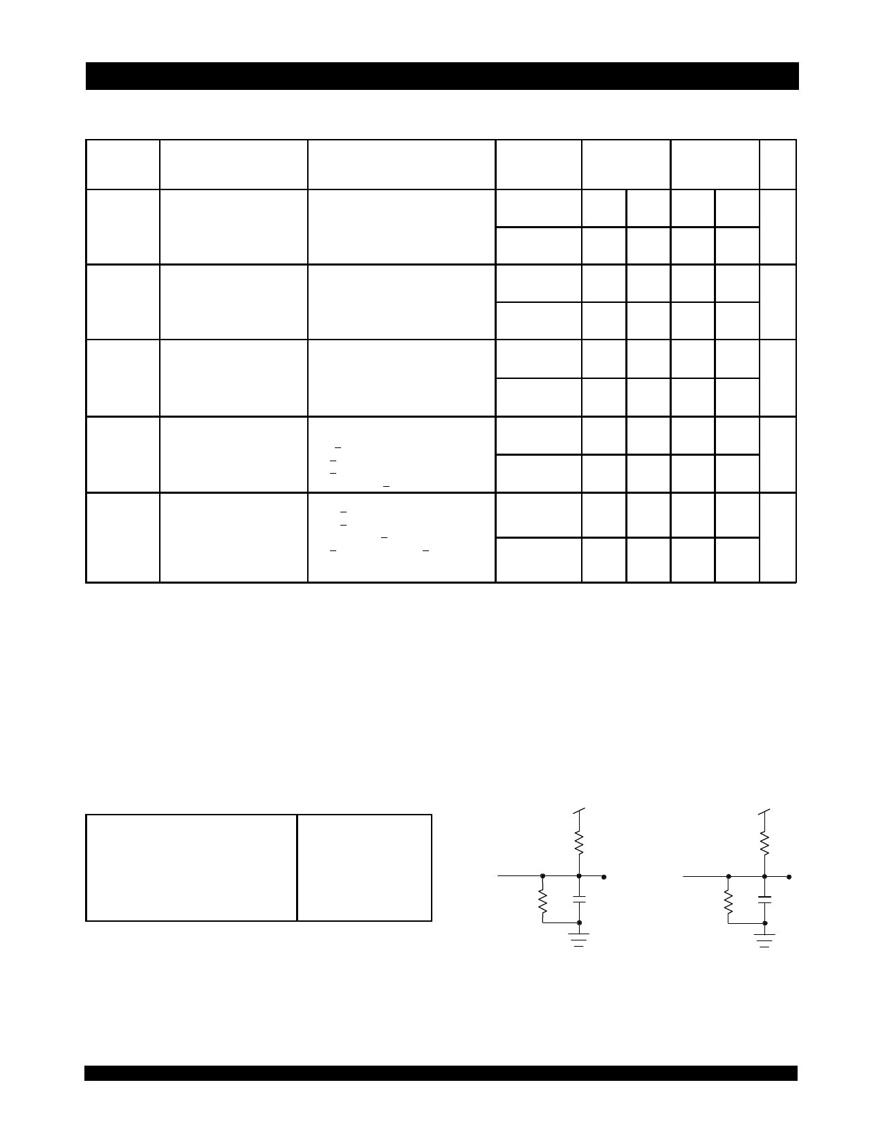
AC Test Conditions
Input Pulse Levels
Input Rise/Fall Times
Input Timing Reference Levels
Output Reference Levels
Output Load
GND to 3.0V
5ns Max.
1.5V
1.5V
Figures 1 and 2
3740 tbl 11
DATAOUT
BUSY
INT
435Ω
3.3V
590Ω
30pF
3740 drw 03
Figure 1. AC Output Load
DATAOUT
435Ω
3.3V
590Ω
5pF
3740 drw 04
Figure 2. Output Test Load
(for tLZ, tHZ, tWZ, tOW)
* Including scope and jig.
6
Share Link: 