IDT74FCT646 데이터 시트보기 (PDF) - Integrated Device Technology
부품명
상세내역
일치하는 목록
IDT74FCT646 Datasheet PDF : 8 Pages
| |||
IDT54/74FCT646/A/C
FAST CMOS OCTAL TRANSCEIVER/REGISTER
MILITARY AND COMMERCIAL TEMPERATURE RANGES
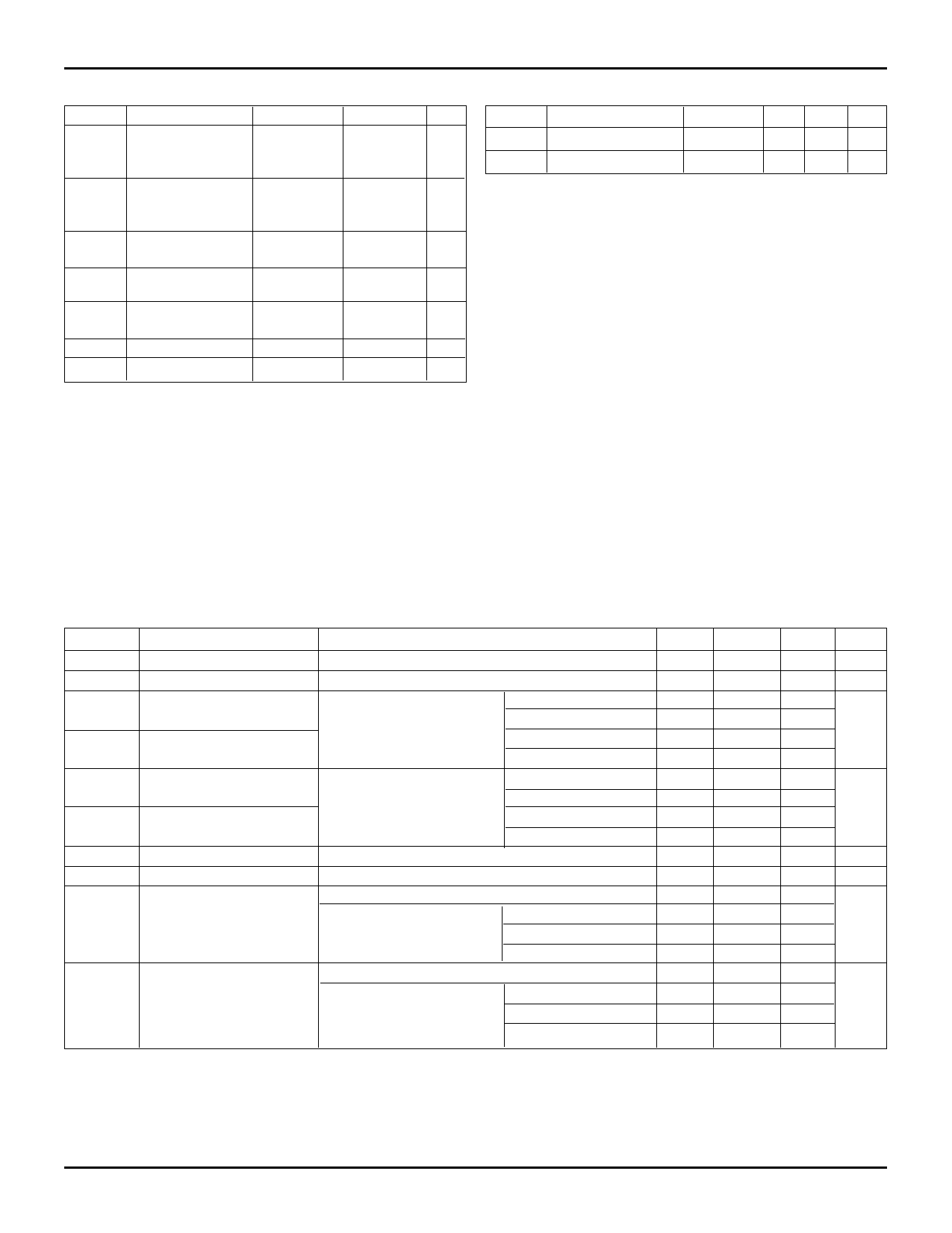
ABSOLUTE MAXIMUM RATINGS(1)
Symbol
Rating
VTERM(2) Terminal Voltage
with Respect
to GND
VTERM(3) Terminal Voltage
with Respect
to GND
Commercial Military Unit
–0.5 to +7.0 –0.5 to +7.0 V
–0.5 to VCC –0.5 to VCC V
TA
Operating
Temperature
0 to +70 –55 to +125 °C
TBIAS
Temperature
Under Bias
–55 to +125 –65 to +135 °C
TSTG
Storage
Temperature
–55 to +125 –65 to +150 °C
PT
Power Dissipation
0.5
0.5
W
IOUT
DC Output Current
120
120
mA
NOTES:
2536 tbl 03
1. Stresses greater than those listed under ABSOLUTE MAXIMUM
RATINGS may cause permanent damage to the device. This is a stress
rating only and functional operation of the device at these or any other
conditions above those indicated in the operational sections of this
specification is not implied. Exposure to absolute maximum rating
conditions for extended periods may affect reliability. No terminal voltage
may exceed VCC by +0.5V unless otherwise noted.
2. Inputs and VCC terminals only.
3. Outputs and I/O terminals only.
CAPACITANCE (TA = +25°C, f = 1.0MHz)
Symbol Parameter(1) Conditions Typ. Max. Unit
CIN
Input Capacitance VIN = 0V
6 10 pF
CI/O
I/O Capacitance
VOUT = 0V 8 12 pF
NOTE:
2536 tbl 04
1. This parameter is measured at characterization but not tested.
DC ELECTRICAL CHARACTERISTICS OVER OPERATING RANGE
Following Conditions Apply Unless Otherwise Specified: VLC = 0.2V; VHC = VCC – 0.2V
Commercial: TA = 0°C to +70°C, VCC = 5.0V ± 5%; Military: TA = –55°C to +125°C, VCC = 5.0V ± 10%
Symbol
Parameter
Test Conditions(1)
Min. Typ.(2)
VIH
Input HIGH Level
Guaranteed Logic HIGH Level
2.0
—
VIL
Input LOW Level
Guaranteed Logic LOW Level
—
—
IIH
Input HIGH Current
VCC = Max.
VI = VCC
—
—
(Except I/O pins)
VI = 2.7V
—
—
IIL
Input LOW Current
VI = 0.5V
—
—
(Except I/O pins)
VI = GND
—
—
IIH
Input HIGH Current
VCC = Max.
VI = VCC
—
—
(I/O pins only)
VI = 2.7V
—
—
IIL
Input LOW Current
VI = 0.5V
—
—
(I/O pins only)
VI = GND
—
—
VIK
Clamp Diode Voltage
VCC = Min., IN = –18mA
IOS
Short Circuit Current
VCC = Max.(3), VO = GND
—
–0.7
–60
–120
VOH
Output HIGH Voltage
VCC = 3V, VIN = VLC or VHC, IOH = –32µA
VHC
VCC
VCC = Min.
IOH = –300µA
VHC
VCC
VIN = VIH or VIL
IOH = –12mA MIL.
2.4
4.0
IOH = –15mA COM’L. 2.4
4.0
VOL
Output LOW Voltage
VCC = 3V, VIN = VLC or VHC, IOL = 300µA
—
GND
VCC = Min.
IOL = 300µA
—
GND
VIN = VIH or VIL
IOL = 48mA MIL.
—
0.3
IOL = 64mA COM’L.
—
0.3
Max.
—
0.8
5
5(4)
–5(4)
–5
15
15(4)
–15(4)
–15
–1.2
—
—
—
—
—
VLC
VLC(4)
0.55
0.55
Unit
V
V
µA
µA
V
mA
V
V
NOTES:
1. For conditions shown as Max. or Min., use appropriate value specified under Electrical Characteristics for the applicable device type.
2. Typical values are at VCC = 5.0V, +25°C ambient and maximum loading.
3. Not more than one output should be shorted at one time. Duration of the short circuit test should not exceed one second.
4. This parameter is guaranteed but not tested.
2536 tbl 05
7.18
4
Share Link: 