ICS9214 데이터 시트보기 (PDF) - Integrated Circuit Systems
부품명
상세내역
일치하는 목록
ICS9214 Datasheet PDF : 16 Pages
| |||
Integrated
Circuit
Systems, Inc.
ICS9214
PLL Multiplier
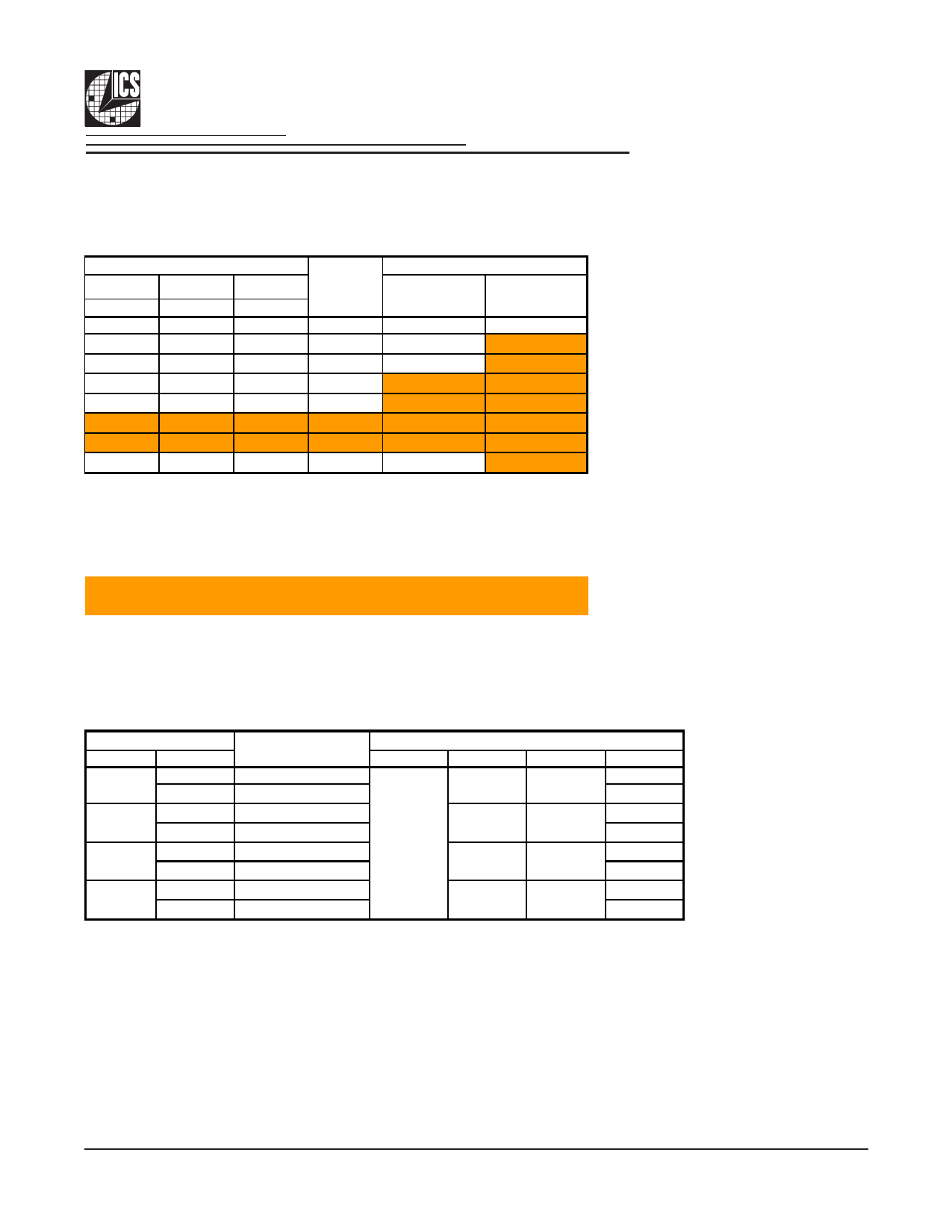
Table 2 shows the frequency multipliers in the PLL, selectable by programming the MULT0, MULT1 and MULT2 bits in the
SMBus Multiplier Control register. Power up default is 4.
Table 2. PLL Multiplier Selection
Byte 0
Bit 6
Bit 5
Bit 4
MULT2
0
0
0
MULT1
0
0
1
MULT0
0
1
0
0
1
1
1
0
0
1
0
1
1
1
0
1
1
1
Frequency
Multiplier
3
4
5
6
8
9/2
15/2
15/4
Output Frequency (MHz)
CLK_INT/C =
100 MHz1
CLK_INT/C =
133 MHz1
3003
400
4002
533
500
667
600
800
800
-3
450
600
750
-3
375
500
NOTES
1 Output frequencies are based on nominal input frequencies of 100 MHz and 133 MHz. The PLL
multipliers are also applicable to spread spectrum modulated input clocks.
2 Default muliplier value at power up
3 Outputs at these settings do not conform to the AC Output Characteristics, or are not supported.
4 Shaded areas are under development and are not yet supported
Device ID and SMBus Device Address
The device ID (SMB_A(1:0)) is part of the SMBus device address. The least significant bit of the address designates a write
or read operation. Table 3 shows the addresses for four ICS9214 devices on the same SMBus.
Table 3. SMBus Device Addresses
ICS9214
Device Operation
Write
0
Read
Hex Address
D8
D9
Write
DA
1
Read
DB
Write
DC
2
Read
DD
Write
DE
3
Read
DF
8-bit SMBus Device Address, Including Oper.
SMB_A1 SMB_A0 WR#/RD
0
0
0
1
0
0
1
1
11011
0
1
0
1
0
1
1
1
0809D—04/07/06
5
Share Link: 