ICS81006I 데이터 시트보기 (PDF) - Integrated Device Technology
부품명
상세내역
일치하는 목록
ICS81006I Datasheet PDF : 14 Pages
| |||
ICS81006I
VCXO-TO-6 LVCMOS OUTPUTS
RECOMMENDATIONS FOR UNUSED INPUT AND OUTPUT PINS
INPUTS:
OUTPUTS:
CONTROL PINS:
All control pins have internal pull-ups or pull-downs; additional
resistance is not required but can be added for additional
protection. A 1kΩ resistor can be used. The VC pin can not be
floated.
LVCMOS OUTPUT:
All unused LVCMOS output can be left floating. We recommend
that there is no trace attached.
SCHEMATIC EXAMPLE
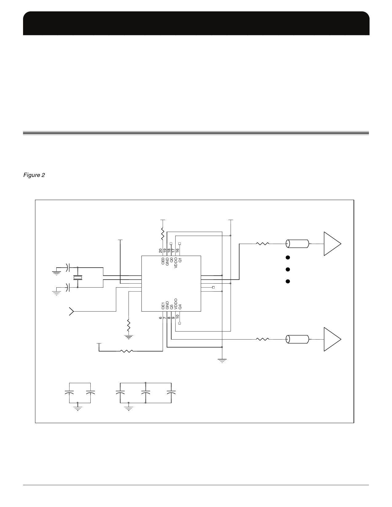
Figure 2 shows an example of ICS81006I application schematic.
The decoupling capacitors should be located as close as
possible to the power pin. For the LVCMOS 20Ω output drivers,
series termination example is shown in the schematic. Additional
termination approaches are shown in the LVCMOS Termination
Application Note.
Quartz crystal should be
placed as close to the
device as possible.
C1
SPARE
VDD
Pull-up VDD
example
R4
1K
U1
VDDO
R1
30
Zo = 50
XTAL
C2
SPARE
VC = 0V to VDD
VC
1
2
3
4
XTAL_IN
XTAL_OUT
VDD
5
VC
DIV_SEL_Q5
Pull-down
example
810068I 1006
R3
1K
VDD
R5 1K
15
GND
Q2
VDDO
14
13
12
Q3
GND
11
R2
Zo = 50
30
(U1-3)
VDD
C7
10uf
C6
0.1uF
(U1-9) (U1-13) (U1-17)
VDDO
C5
0.1uF
C4
0.1uF
C3
0.1uF
Unused outputs can be left floating. There should be
no trace attached to unused outputs. Device
characterized and specification limits set with all
outputs terminated.
FIGURE 2. ICS81006I SCHEMATIC EXAMPLE
IDT™ / ICS™ VCXO-TO-LVCMOS OUTPUTS
10
ICS81006AKI REV A OCTOBER 2, 2006
Share Link: 