MP7652 데이터 시트보기 (PDF) - Exar Corporation
부품명
상세내역
일치하는 목록
MP7652 Datasheet PDF : 16 Pages
| |||
MP7652
THEORY OF OPERATION
The MP7652 is a 4-channel multiplying D/A converter that in-
corporates a novel open loop architecture invented by MPS.
The design produces the widest bandwidth, fastest settling time,
most constant group delay, and a very low noise operation
compared to the conventional R-2R based architectures (given
an equal technology platform). This device is particularly useful
in applications where analog multipliers are used to perform the
gain adjustment function for high frequency analog signal condi-
tioning. Analog multipliers produce much higher noise and.
This design allows for digital control of gain with constant and
very low noise for all gain settings.
Linearity Characteristics
Each DAC achieves DNL +0.5 LSB (typ), INL +1 LSB
(typ), and gain error +1.5%. Since all 4 channel D/A convert-
ers are fabricated on the same IC, the linearity matching and
gain matching of +0.5% (typ) is achieved.
AC and Low Noise Performance
The novel subranging architecture delivers a 15 MHz (type)
–3 dB bandwidth. A constant group delay of 70 ns (typ) is
achieved to frequencies up to 8 MHz. Analog output settling
time for a code change of FS to ZS and ZS to FS with VREFP = 3
V, is typically 150 ns (with RL = 5 k to VEE). Also, with all codes
set to FS (all 1s) and a VREFP 3 V step, the analog output will
settle to 8 bits in less than 110 ns (typ). Note that the AC perfor-
mance specifications also match to between all 4 channels. The
above AC and transient performance is achieved with each
channel consuming only 20 mW (typ) with 10 V p-p supplies.
Serial Port
MP7652 is equipped with a serial data 3-wire standard µ-proc-
essor logic interface to reduce pin count, package size, and
board wire (space). This interface consists of LD which controls
the transfer of data to the selected DAC channel, SDI (serial
data/address input), CLK (shift register clock) and SDO (serial
data output). When the LD signal is high, CLK signal loads the
digital input bits (SDI) into the 12-bit shift register. The LD signal
going low loads this data into the selected DAC. The LD signal
going low also disables the serial data input (SDI), output (SDO
tri-stated) and the CLK input. This design tremendously re-
duces digital noise, and glitch transients into the DACs due to
free running CLK and SDI. Also, tri-stating the SDO output with
LD signal would allow read back of pre-stored digital data of the
selected package using one SDO wire for all DAC ICs on the
board. When the PRESET signal is low, the output of all DACs
are 1/2 of (VREFP + VREFN), regardless of any digital inputs.
Note that VREFP is referenced to VREFN.
Power Supplies and Voltage Reference DC Voltage
Ranges
For the single supply operation, VCC = +10 V, VDD = +5 V, and
VEE = DGND = 0 V. The VO 1-4 and VREFP 1-4 range would be
VCC –1.8 V (10 – 1.8 = 8.2 V) to VEE +1.5 V (0 + 1.5 = 1.5 V).
VREFN is the equivalent of AGND for this DAC. In this mode
VREFN can be set at (VCC + VEE)/2 = (10 + 0)/2 = 5 V. VREFN 1-4
DC range can also be set from VEE +1.5 = 1.5 V to VCC – 1.5 =
8.2 V. Refer to Table 2. for the relationship equations.
For the dual supply operation, VCC = +5, VDD = +5, and VEE =
–5 V. The VOUT 1-4 and VREFP 1-4 range would be VCC –1.8 V
(–1.8 = 3.2 V) to VEE +1.5 V (–5 + 1.5 = –3.5 V). In this mode
VREFN can be set to (VCC + VEE)/2 = (5 – 5)/2 = 0 V. Similarly,
VREFN 1-4 DC range can be set from VEE +1.5 V = 3.5 V to VCC
–1.8 = +3.2 V. Refer to Table 2. for the relationship equations.
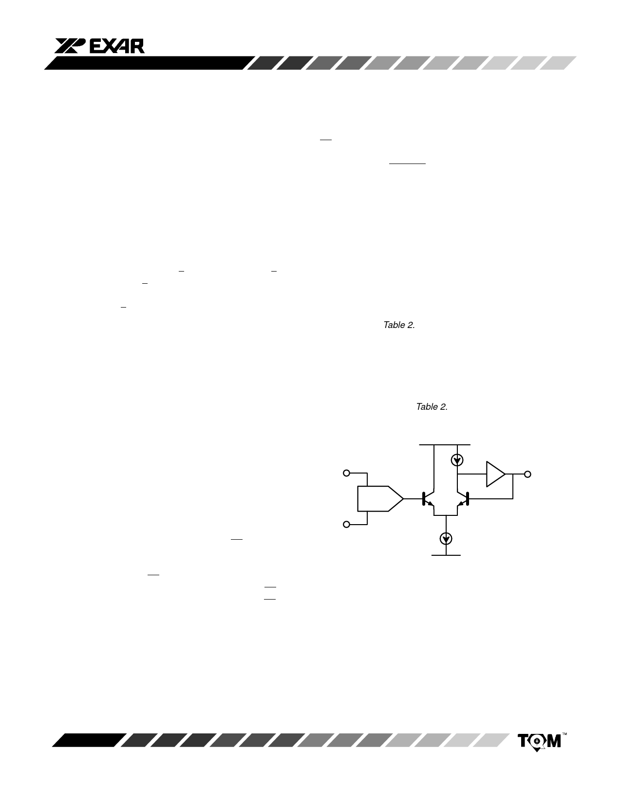
VREFP 1-4
DAC
VCC
+1
Q2 Q1
VOUT 1-4
VREFN 1-4
I1
VEE
Figure 4. Simplified Block Diagram
Rev. 1.00
7
Share Link: 