MP7652 데이터 시트보기 (PDF) - Exar Corporation
부품명
상세내역
일치하는 목록
MP7652 Datasheet PDF : 16 Pages
| |||
MP7652
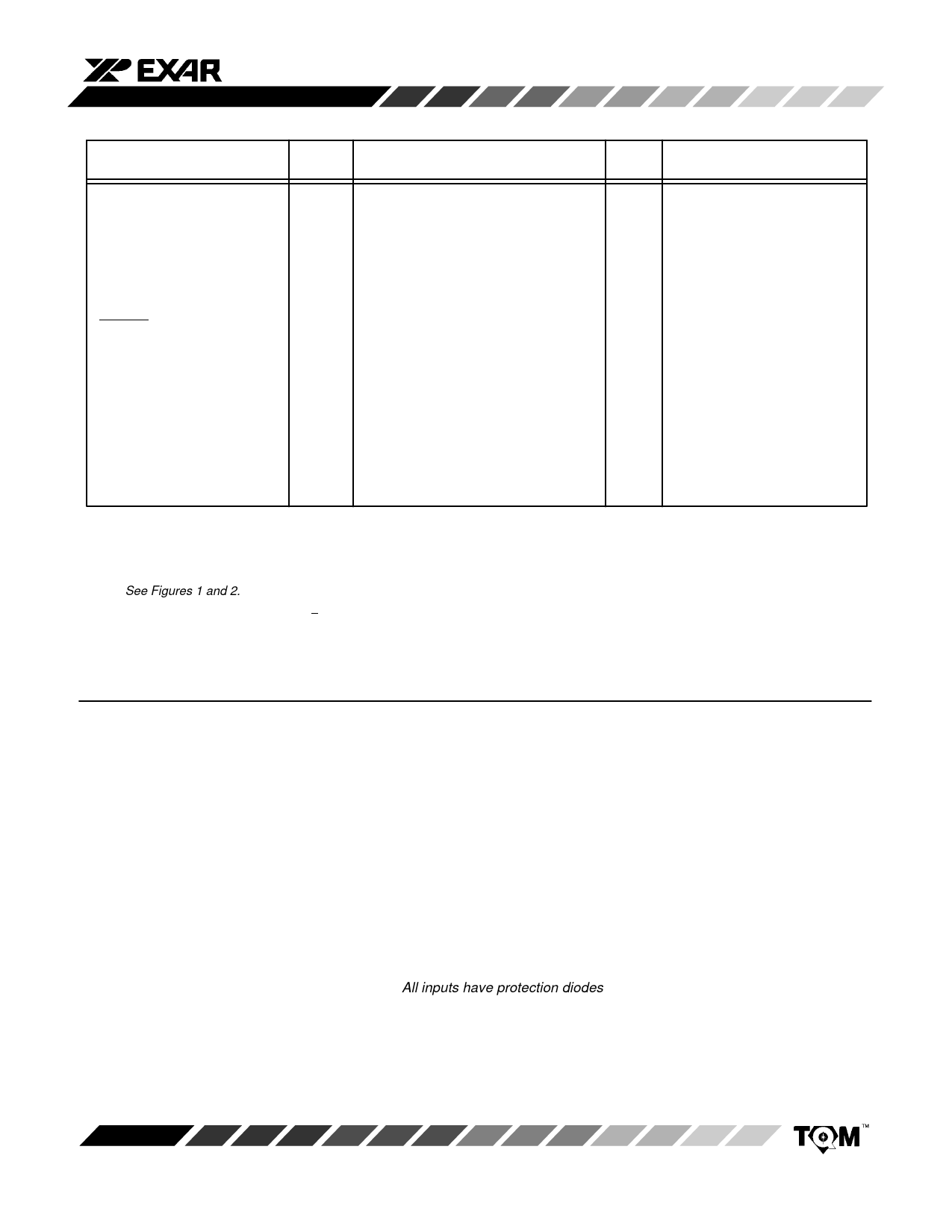
ELECTRICAL CHARACTERISTICS TABLE
Description
Symbol
Min
DIGITAL TIMING
SPECIFICATIONS2, 4
Input Clock Pulse Width
tCH, tCL
60
Data Setup Time
tDS
70
Data Hold Time
tDH
0
CLK to SDO Propagation Delay
tPD
DAC Register Load Pulse Width
tLD
100
PRESET Pulse Width
tPR
50
Clock Edge to Load Rising Edge
tCKLD1
100
Clock Edge to Load Falling Edge tCKLD2
0
Load Falling Edge to SDO
tHZ1
80
Tri-state Enable
Load Rising Edge to SDO
Tri-state Disable
tHZ2
40
Load Falling Edge to CLK Disable tLDCK1
30
Load Rising Edge to CLK Enable tLDCK2
60
LD Set-up Time with Respect
tLDSU
20
to CLK
25°C
Typ
Max
Units Conditions
ns
ns
ns
150
ns
ns
ns
ns
ns
ns
ns
ns
ns
ns
NOTES
1 Full Scale Range (FSR) is 3V.
2 Guaranteed but not production tested.
3 Digital input levels should not go below ground or exceed the positive supply voltage, otherwise damage may occur.
4 See Figures 1 and 2.
5 For reference input pulse: tR = tF > 100 ns.
Specifications are subject to change without notice
ABSOLUTE MAXIMUM RATINGS (TA = +25°C unless otherwise noted)1, 2
VCC to VREFN . . . . . . . . . . . . . . . . . . . . . . . . . . . . . . . . . +6.5 V
VEE to VREFN . . . . . . . . . . . . . . . . . . . . . . . . . . . . . . . . . –6.5 V
VCC to DGND . . . . . . . . . . . . . . . . . . . . . . . . . . . . . . . . +13.0 V
VEE to DGND . . . . . . . . . . . . . . . . . . . . . . . . . . . . . . . . . –6.5 V
VREFP 1-4 to DGND, VREFN . . . . . . . . . . . . . . . . . VCC to VEE
Digital Input & Output Voltage to DGND –0.5 to VDD +0.5 V
Operating Temperature Range
Extended Industrial . . . . . . . . . . . . . . . . . . . –40°C to +85°C
Maximum Junction Temperature . . . . . . . . . –65°C to 150°C
Storage Temperature . . . . . . . . . . . . . . . . . . . . . . . . . . 150°C
Lead Temperature (Soldering, 10 sec) . . . . . . . . . . . +300°C
Package Power Dissipation Rating @ 75°C
PDIP, SOIC . . . . . . . . . . . . . . . . . . . . . . . . . . . . . 1000mW
Derates above 75°C . . . . . . . . . . . . . . . . . . . . . . 6mW/°C
NOTES:
1 Stresses above those listed under “Absolute Maximum Ratings” may cause permanent damage to the device. This is a
stress rating only and functional operation at or above this specification is not implied. Exposure to maximum rating
conditions for extended periods may affect device reliability.
2 Any input pin which can see a value outside the absolute maximum ratings should be protected by Schottky diode clamps
(HP5082-2835) from input pin to the supplies. All inputs have protection diodes which will protect the device from short
transients outside the supplies of less than 100mA for less than 100µs.
Rev. 1.00
5
Share Link: 