FM24C32 데이터 시트보기 (PDF) - Fairchild Semiconductor
부품명
상세내역
일치하는 목록
FM24C32 Datasheet PDF : 13 Pages
| |||
Write Operations
BYTE WRITE
For byte write operation, two bytes of address are required after
the slave address. These two bytes select 1 out of the 4096
locations in the memory. The master provides these two address
bytes and for each address byte received, FM24C32U responds
with an acknowledge pulse. Master then provides a byte of data
to be written into the memory. Upon receipt of this data, FM24C32U
responds with an acknowledge pulse. The master then terminates
the transfer by generating a stop condition, at which time the
FM24C32U begins the internal write cycle to the memory. While
the internal write cycle is in progress the FM24C32U inputs are
disabled, and the device will not respond to any requests from the
master for the duration of tWR. Refer Figure 4 for the address,
acknowledge and data transfer sequence.
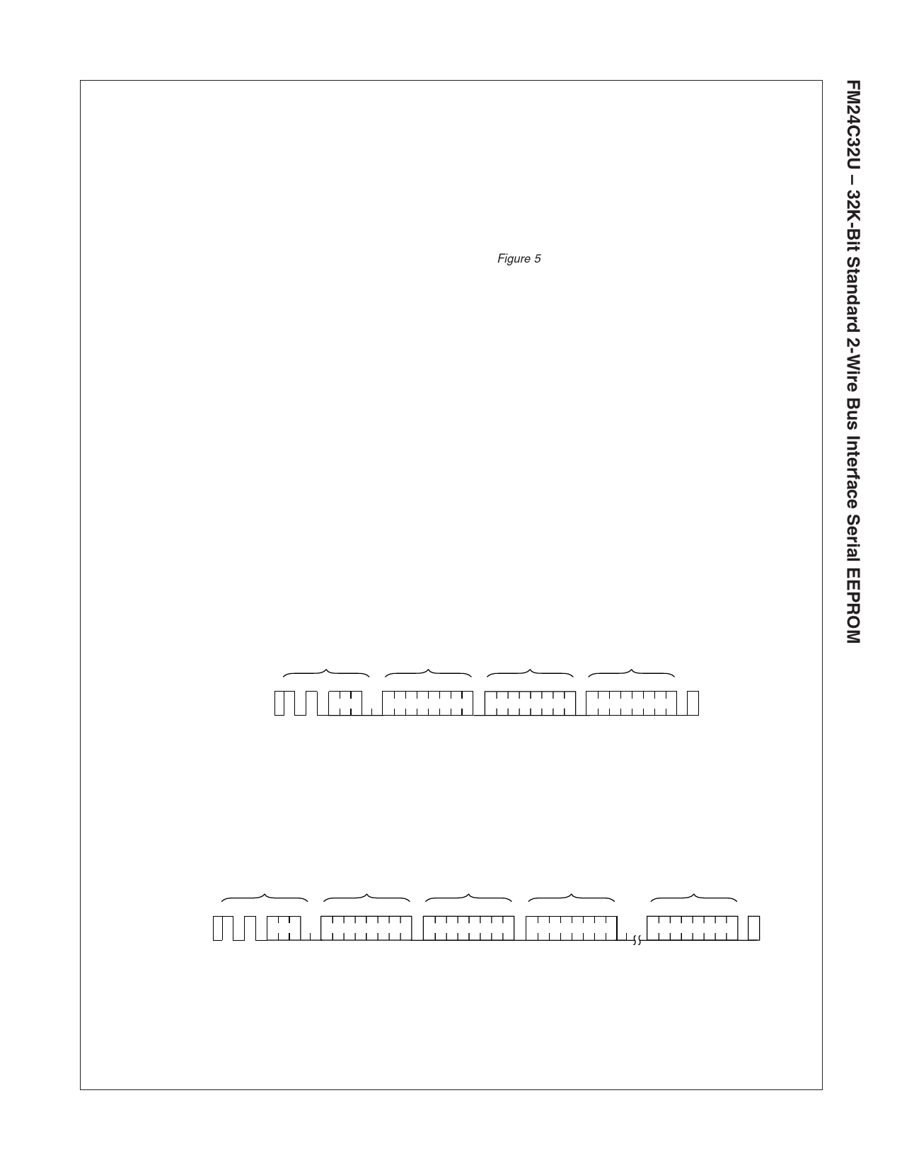
PAGE WRITE
To minimize write cycle time, FM24C32U offers Page Write
feature, which allows simultaneous programming of up to 32
contiguous bytes. To facilitate this feature, the memory array is
organized in terms of “Pages”. A Page consists of 32 contiguous
byte locations starting at every 32-Byte address boundary (for
example, starting at array address 0x0000, 0x0020, 0x0040 etc.).
Page Write operation is confined to a single page. In other words
a Page Write operation will not cross over to locations on the next
page but will “roll over” to the beginning of the same page
whenever end of page is reached and additional data bytes are a
continued to be provided. A Page Write operation can be initiated
to begin at any location within a page (starting address of the Page
Write operation need not be the starting address of a Page).
Page Write is initiated in the same manner as the Byte Write
operation; but instead of terminating the cycle after transmitting
the first data byte, the master can further transmit up to 31 more
bytes. After the receipt of each byte, FM24C32U will respond with
an acknowledge pulse, increment the internal address counter to
the next address, and is ready to accept the next data. If the master
should transmit more than 32 bytes prior to generating the STOP
condition, the address counter will “roll over” and previously
loaded data will be re-loaded. As with the Byte Write operation, all
inputs are disabled until completion of the internal write cycle.
Refer Figure 5 for the address, acknowledge, and data transfer
sequence.
Acknowledge Polling
Once the stop condition is issued to indicate the end of the host’s
write operation, the FM24C32U initiates the internal write cycle.
ACK polling can be initiated immediately. This involves issuing the
start condition followed by the slave address for a write operation.
If the FM24C32U is still busy with the write operation, no ACK will
be returned. If the FM24C32U has completed the write operation,
an ACK will be returned and the host can then proceed with the
next read or write operation.
Write Protection
Programming of the upper half (upper 8Kbit) of the memory will not
take place if the WP pin of the FM24C32U is connected to VCC.
The FM24C32U will respond to slave and byte addresses; but if
the memory accessed is write protected by the WP pin, the
FM24C32U will not generate an acknowledge after the first byte
of data has been received. Thus the program cycle will not be
started when the stop condition is asserted.
Byte Write (Figure 4)
Page Write (Figure 5) S
T
Bus Activity: A
Master R
T
SLAVE
ADDRESS
WORD
ADDRESS (1)
WORD
ADDRESS (0)
DATA
S
T
O
P
SDA Line
Bus Activity:
EEPROM
A
A
A
A
C
C
C
C
K
K
K
K
S
T
Bus Activity: A
Master R
T
SDA Line
SLAVE
ADDRESS
Bus Activity:
EEPROM
WORD
ADDRESS (1)
WORD
ADDRESS (0)
A
A
A
C
C
C
K
K
K
DATA n
A
C
K
DATA n+31
S
T
O
P
A
C
K
FM24C32U Rev. A.1
10
www.fairchildsemi.com
Share Link: 