EM4022V16WS11 데이터 시트보기 (PDF) - EM Microelectronic - MARIN SA
부품명
상세내역
일치하는 목록
EM4022V16WS11
EM Microelectronic - MARIN SA

EM4022V16WS11 Datasheet PDF : 15 Pages
| |||
Power storage capacitor calculation
The global current consumption of the device defines the
external storage capacitor.
When the device modulate, the supply voltage is picked
from the supply capacitor and should never decrease
under the falling edge of the power on reset (VPONF). If
this occurs, the device goes in a reset mode and any
data transmission is aborted. The worst case for the
storage capacitor calculation is when the device is put in
the electromagnetic field. At this moment the supply
reaches the VPONR and start to modulate. During
modulation the power store in the capacitor must be high
enough so that at the end of the modulation the supply is
higher than VPORF.. This means that the voltage reduction
on the capacitor must be less than the hysteresis of the
power on reset (VPHYS).
And this when the chip has a supply voltage of around
the power on reset threshold
The total current consumption from the storage capacitor
is defined by the modulation current IMOD,
This current is the consumption of the power on reset
block, oscillator and the logic which work at a typical
frequency of 125KHz. The GAP current is also included
in this parameter.
The duration where this currents is present for the
capacitor calculation, is dependent of the data rate
EM4022
Calculation example :
Below we define typical cases combinations :
FOSC = 125 KHz
VPHYS = 120 mV
IMOD = 9 µA
Data rate is 4 KBaud.
CPx
=
I MOD *128 *103
FOSC *VHYS * BaudRate
=
9 *10−6 *128 *103
125*103 *160 *10−3 * 4 *103
= 14.4nF
Of course, this value can be adapted to the
electromagnetic power and to the performances that
must be achieved. If a tag is put in a field within a short
time, the emitting power must be high enough to charge
up the capacitor.
The chip integrates a 140pF supply capacitor.
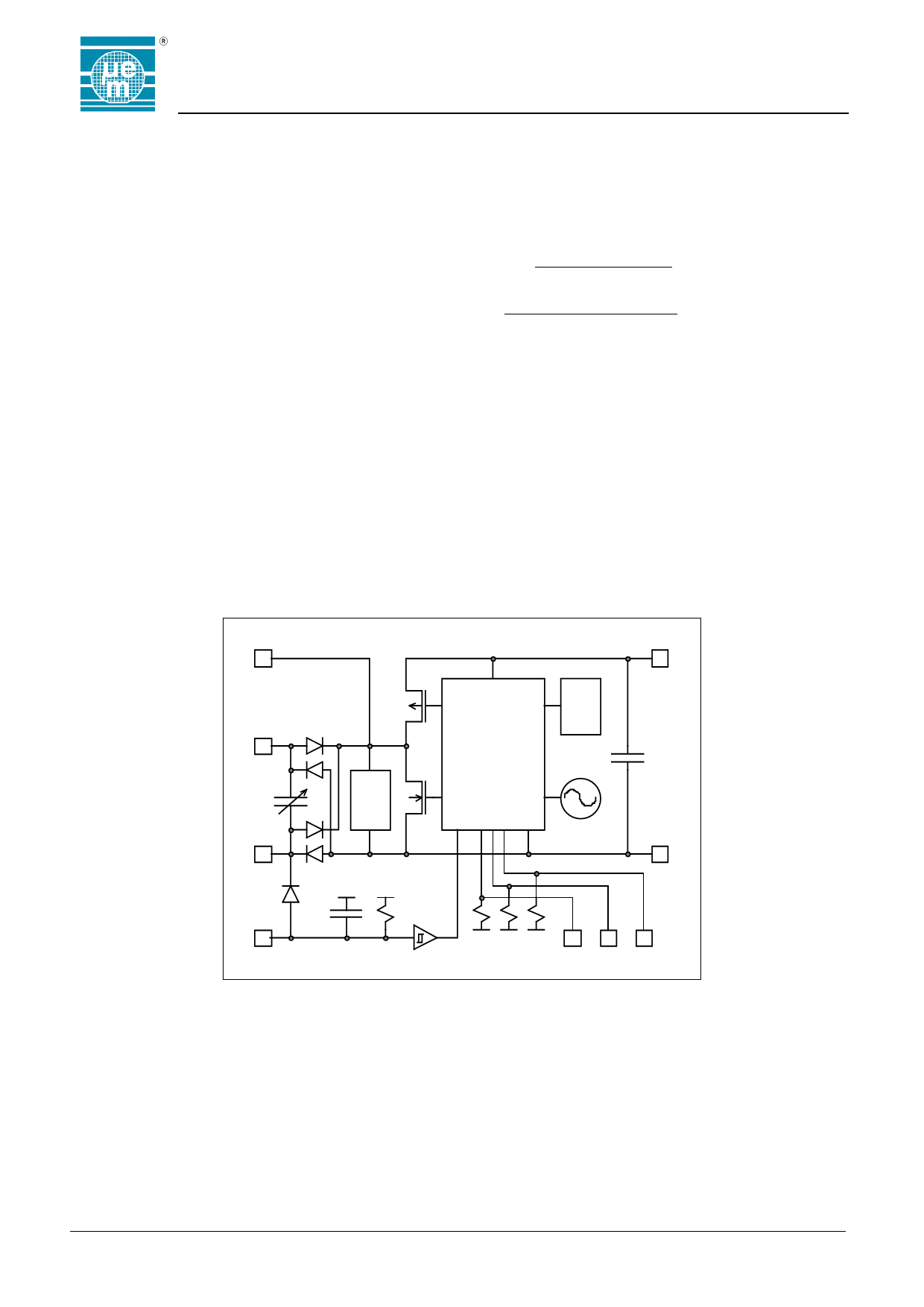
Block Diagram
M
VDD
COIL1
D2
P
Q1
VDD
R
LOGIC
PON
D4
CR
Shunt
N
C
D3
COIL2
Q2 GAP TST VSS
OSC
CP
VSS
GAP
D1
DG VDD
CG
VDD
RG
VSS VSS VSS
SI XCLK TMC
Fig. 5
Copyright 2002, EM Microelectronic-Marin SA
4
www.emmicroelectronic.com
Share Link: