CY7C4425-35AI 데이터 시트보기 (PDF) - Cypress Semiconductor
부품명
상세내역
일치하는 목록
CY7C4425-35AI Datasheet PDF : 25 Pages
| |||
CY7C4425/4205/4215
CY7C4225/4235/4245
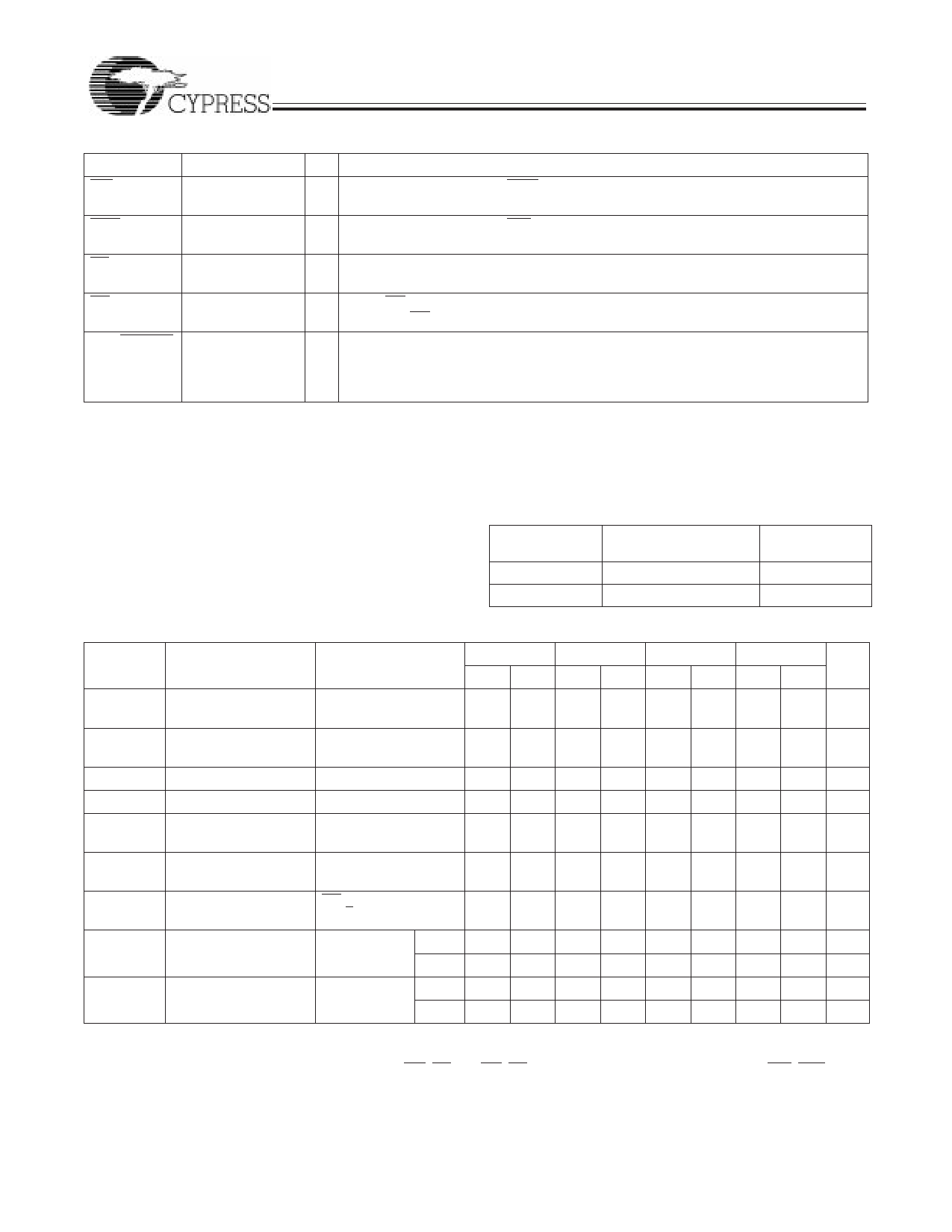
Pin Definitions (continued)
Signal Name Description
RXI
Read Expansion
Input
RXO
Read Expansion
Output
RS
Reset
OE
Output Enable
VCC/SMODE Synchronous
Almost Empty/
Almost Full Flags
I/O
Function
I Cascaded - Connected to RXO of previous device.
Not Cascaded - Tied to VSS.
O Cascaded - Connected to RXI of next device.
I Resets device to empty condition. A reset is required before an initial read or write
operation after power-up.
I When OE is LOW, the FIFO’s data outputs drive the bus to which they are con-
nected. If OE is HIGH, the FIFO’s outputs are in High Z (high-impedance) state.
I Dual-Mode Pin
Asynchronous Almost Empty/Almost Full flags - tied to VCC.
Synchronous Almost Empty/Almost Full flags - tied to VSS.
(Almost Empty synchronized to RCLK, Almost Full synchronized to WCLK.)
Maximum Ratings
Output Current into Outputs (LOW)............................. 20 mA
(Above which the useful life may be impaired. For user guide-
lines, not tested.)
Storage Temperature ....................................−65°C to +150°C
Static Discharge Voltage ........................................... >2001V
(per MIL-STD-883, Method 3015)
Latch-Up Current ..................................................... >200 mA
Ambient Temperature with
Power Applied.................................................−55°C to +125°C
Supply Voltage to Ground Potential .................−0.5V to +7.0V
DC Voltage Applied to Outputs
in High Z State .....................................................−0.5V to +7.0V
DC Input Voltage .................................................−3.0V to +7.0V
Operating Range
Range
Commercial
Industrial[1]
Ambient
Temperature
0°C to +70°C
−40°C to +85°C
VCC
5V ± 10%
5V ± 10%
Electrical Characteristics Over the Operating Range[2]
7C42X5-10 7C42X5-15 7C42X5-25 7C42X5-35
Parameter
Description
Test Conditions Min. Max. Min. Max. Min. Max. Min. Max. Unit
VOH
VOL
VIH[3]
VIL[3]
IIX
IOS[4]
IOZL
IOZH
ICC2[5]
ISB[6]
Output HIGH Voltage
Output LOW Voltage
Input HIGH Voltage
Input LOW Voltage
VCC = Min.,
IOH = −2.0 mA
VCC = Min.,
IOL = 8.0 mA
2.4
2.4
2.4
2.4
V
0.4
0.4
0.4
0.4 V
2.2 VCC 2.2 VCC 2.2 VCC 2.2 VCC V
−3.0 0.8 −3.0 0.8 −3.0 0.8 −3.0 0.8 V
Input Leakage
Current
VCC = Max.
−10 +10 −10 +10 −10 +10 −10 +10 µA
Output Short
Circuit Current
Output OFF,
High Z Current
Operating Current
VCC = Max.,
VOUT = GND
−90
−90
−90
−90
mA
OE > VIH,
VSS < VO < VCC
−10 +10 −10 +10 −10 +10 −10 +10 µA
VCC = Max., Com’l
45
45
45
45 mA
IOUT = 0 mA Ind
50
50
50
50 mA
Standby Current
VCC = Max., Com’l
10
10
10
10 mA
IOUT = 0 mA Ind
15
15
15
15 mA
Notes:
1. TA is the “instant on” case temperature.
2. See the last page of this specification for Group A subgroup testing information.
3. The VIH and VIL specifications apply for all inputs except WXI, RXI. The WXI, RXI pin is not a TTL input. It is connected to either RXO, WXO of the
previous device or VSS.
4. Test no more than one output at a time for not more than one second.
5. Input signals switch from 0V to 3V with a rise/fall time less than 3 ns, clocks and clock enables switch at 20 MHz, while the data inputs switch at 10 MHz.
Outputs are unloaded.
6. All input signals are connected to VCC. All outputs are unloaded.
4
Share Link: 