CXD2453Q 데이터 시트보기 (PDF) - Sony Semiconductor
부품명
상세내역
일치하는 목록
CXD2453Q Datasheet PDF : 21 Pages
| |||
CXD2453Q
Description of Operation
• Sync signal input pins (HSYNC, VSYNC)
Horizontal and vertical separate SYNC signals are input to the HSYNC (Pin 29) and VSYNC (Pin 28). The
sync signals are compatible with both positive and negative polarity according to serial data settings. (Refer to
the section on serial data interface for details regarding serial data.)
The CXD2453Q supports signals which are shown in the following table.
Effective dots
Horizontal scanning Vertical scanning
frequency
frequency
1024 × 768 (XGA) 44kHz to 69kHz 55Hz to 85Hz
1280 × 1024 (S-XGA)
≤ 69kHz
Roughly ≤ 65Hz
Remarks
Scanning line conversion from 1024 to 768
vertical lines
In the case of signals defined by special protocols that do not satisfy the conditions in the diagram below, it
may not be possible to obtain a complete display even for the above signals when the image display position is
properly set on the LCD panel. This IC does not support interlace signals.
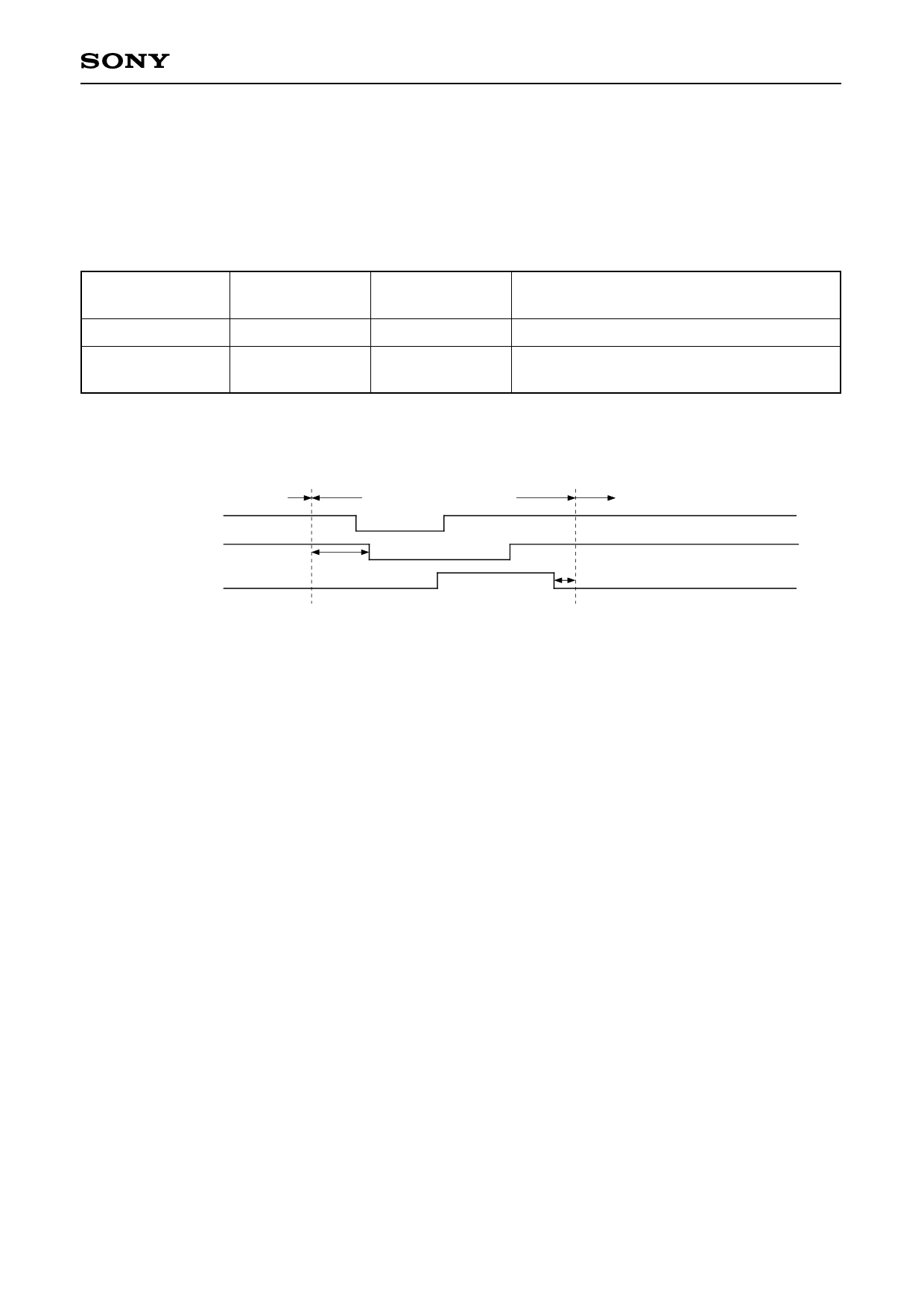
Image display period
HSYNC
ENB
Min. 0.72µs
PCG
Horizontal blanking period
Image display period
Min. 0.17µs
• Master clock input pins (CKI1/XCKI1, CKI2, CKI3/XCKI3, CKI4) and Clock Selection Pins (SLCK1, SLCK2)
Since this IC does not contain a built-in phase comparator, phase comparison is performed externally and a
divided clock is input. The 1/N (N is the clock number during 1 horizontal period) frequency divider output is
output from the HRET (Pin 38) for the external phase comparator.
The clock input pin consists of two channels for small amplitude differential input (center level: 2.0V, amplitude:
±0.4V), and two channels for CMOS level input for a total of four channels. These are selected according to
the SLCK1 (Pin 26), SLCK2 (Pin 30) and serial data.
(1) During normal operation (serial data SLLAP = 0)
All internal circuits of the IC operate with CKI1 or CKI2. CKI1/XCKI1 are selected when SLCK1 = L (Pins
3/4, small amplitude differential input), and CKI2 is selected when SLCK1 = H (Pin 11, CMOS level input).
(2) When using scan converter (serial data SLLAP = 1)
This is used when the input signal clock and output signal clock are different such as when performing
dot conversion using a scan converter. Only the serial data interface and PLL counter of the IC internal
circuits operate with CKI1 or CKI2 (clock synchronized with input signal). All other blocks operate with
CKI3 or CKI4 (output signal clock). CKI3/XCKI13 are selected when SLCK2 = L (Pins 21/22, small
amplitude differential input), and CKI4 is selected when SLCK2 = H (Pin 13, CMOS level input).
• Internal frequency divider reset selection pin (SLHR)
This selects whether reset of the PLL counter (loop counter) with HSYNC is to be enabled or disabled. In the
case of performing phase comparison of the HSYNC and HRET pulses with an external phase comparator, the
SLHR (Pin 17) is set to H (reset disabled). When phase comparison and frequency division are performed
externally and HRET pulses for phase comparison are not used, the SLHR is set to L (reset enabled). At this
time, the output of each pulse is delayed by approximately 8 clocks as compared with using HRET pulses for
phase comparison.
• Signal inversion type selection pin (SLFR)
This selects the inversion cycle of the polarity inversion pulse (FRP pulse) for AC driving. Setting the SLFR
(Pin 19) to H results in field inversion, while setting the SLFR to L results in line inversion.
–9–
Share Link: 