CXD2453Q 데이터 시트보기 (PDF) - Sony Semiconductor
부품명
상세내역
일치하는 목록
CXD2453Q Datasheet PDF : 21 Pages
| |||
CXD2453Q
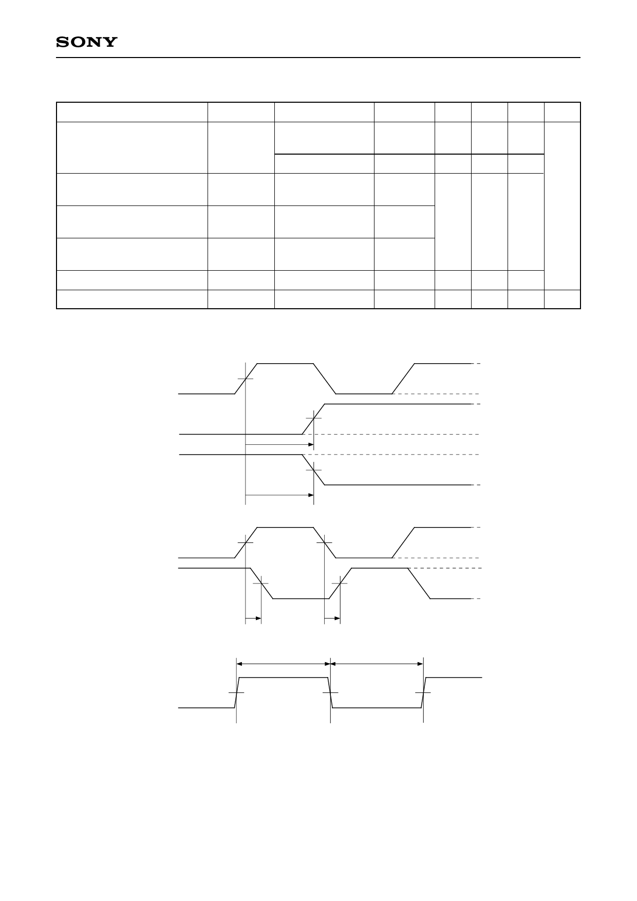
• AC characteristics
Item
Clock input cycle
Output rise/fall delay time
Output rise/fall delay time
Output rise/fall delay time
Cross-point time difference
Duty ratio
Symbol
—
(Topr = –20 to +75°C, VDD = 3.3V ± 0.3V, VSS = 0V)
Applicable pins Conditions Min. Typ. Max. Unit
CKI1/XCKI1,
CKI3/XCKI3
CKI2, CKI4
—
10.5 — —
—
10.5 — —
tpr/tpf
tpr/tpf
HCK1, HCK2, HST CL = 90pF
ns
VCK, BLK, VST,
ENB, PCG
CL = 50pF —
—
25
tpr/tpf
Other output pins CL = 30pF
∆t
HCK1, HCK2
tH/ (tH + tL) HCK1, HCK2
CL = 90pF –5 —
5
CL = 90pF 48 50 52 %
Timing Definitions
VDD
CKI1, CKI2,
CKI3, CKI4
50%
0V
VDD
Output
50%
0V
tpr
VDD
Output
50%
0V
tpf
VDD
HCK1
50%
50%
0V
VDD
HCK2
50%
50%
0V
∆t
∆t
HCK1, HCK2
tH
50%
tL
50%
50%
–6–
Share Link: 