CS51411GMNR2G(2013) 데이터 시트보기 (PDF) - ON Semiconductor
부품명
상세내역
일치하는 목록
CS51411GMNR2G
(Rev.:2013)
(Rev.:2013)
ON Semiconductor

CS51411GMNR2G Datasheet PDF : 20 Pages
| |||
CS51411, CS51412, CS51413, CS51414
independent of switching duty cycle. The maximum load
current, given by the following formula under continuous
conduction mode, is less than the Current Limit due to the
ripple current.
IO(MAX)
+
ILIM
*
VO(VIN * VO)
2(L)(VIN)(fs)
where:
fS = switching frequency,
ILIM = current limit threshold,
VO = output voltage,
VIN = input voltage,
L = inductor value.
When the regulator runs undercurrent limit, the
subharmonic oscillation may cause low frequency
oscillation, as shown in Figure 13. Similar to current mode
control, this oscillation occurs at the duty cycle greater than
50% and can be alleviated by using a larger inductor value.
The current limit threshold is reduced to Foldback Current
when the FB pin falls below Foldback Threshold. This
feature protects the IC and external components under the
power up or overload conditions.
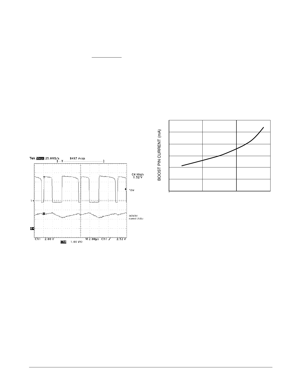
Figure 13. The Regulator in Current Limit
BOOST Pin
The BOOST pin provides base driving current for the
power switch. A voltage higher than VIN provides required
headroom to turn on the power switch. This in turn reduces
IC power dissipation and improves overall system
efficiency. The BOOST pin can be connected to an external
boost−strapping circuit which typically uses a 0.1 mF capacitor
and a 1N914 or 1N4148 diode, as shown in Figure 1. When the
power switch is turned on, the voltage on the BOOST pin is
equal to
VBOOST + VIN ) VO * VF
where:
VF = diode forward voltage.
The anode of the diode can be connected to any DC voltage
other than the regulated output voltage. However, the
maximum voltage on the BOOST pin shall not exceed 40 V.
As shown in Figure 14, the BOOST pin current includes a
constant 7.0 mA predriver current and base current
proportional to switch conducting current. A detailed
discussion of this current is conducted in Thermal
Consideration section. A 0.1 mF capacitor is usually adequate
for maintaining the Boost pin voltage during the on time.
BIAS Pin (CS51412 and CS51414 Only)
The BIAS pin allows a secondary power supply to bias the
control circuitry of the IC. The BIAS pin voltage should be
between 3.3 V and 6.0 V. If the BIAS pin voltage falls below
that range, use a diode to prevent current drain from the
BIAS pin. Powering the IC with a voltage lower than the
regulator’s input voltage reduces the IC power dissipation
and improves energy transfer efficiency.
30
25
20
15
10
5
00
0.5
1.0
1.5
SWITCHING CURRENT (A)
Figure 14. The Boost Pin Current Includes 7.0 mA
Predriver Current and Base Current when the Switch
is Turned On. The Beta Decline of the Power Switch
Further Increases the Base Current at High
Switching Current
Shutdown
The internal power switch will not turn on until the VIN
pin rises above the Startup Voltage. This ensures no
switching until adequate supply voltage is provided to the
IC. The IC transitions to sleep mode when the SHDNB pin
is pulled low. In sleep mode, the internal power switch
transistor remains off and supply current is reduced to the
Shutdown Quiescent Current value (20 mA typical). This pin
has an internal pull-up current source, so defaults to high
(enabled) state when not connected.
http://onsemi.com
10
Share Link: