CS51411GMNR2G(2013) 데이터 시트보기 (PDF) - ON Semiconductor
부품명
상세내역
일치하는 목록
CS51411GMNR2G
(Rev.:2013)
(Rev.:2013)
ON Semiconductor

CS51411GMNR2G Datasheet PDF : 20 Pages
| |||
CS51411, CS51412, CS51413, CS51414
VIN
I1
5mA
Q2
To internal
bias rails
SHDNB
(a)
20k
Q1
D1
8V
0.65V
SHDNB
Z1
(b)
2V to 5V
(c)
SHDNB
where:
VC = VC pin steady−state voltage, which is approximately
equal to error amplifier’s reference voltage.
CCOMP = Compensation capacitor connected to the VC pin
ISOURCE = Output Source Current of the error amplifier.
Using a 0.1 mF CCOMP, the calculation shows a TSS over
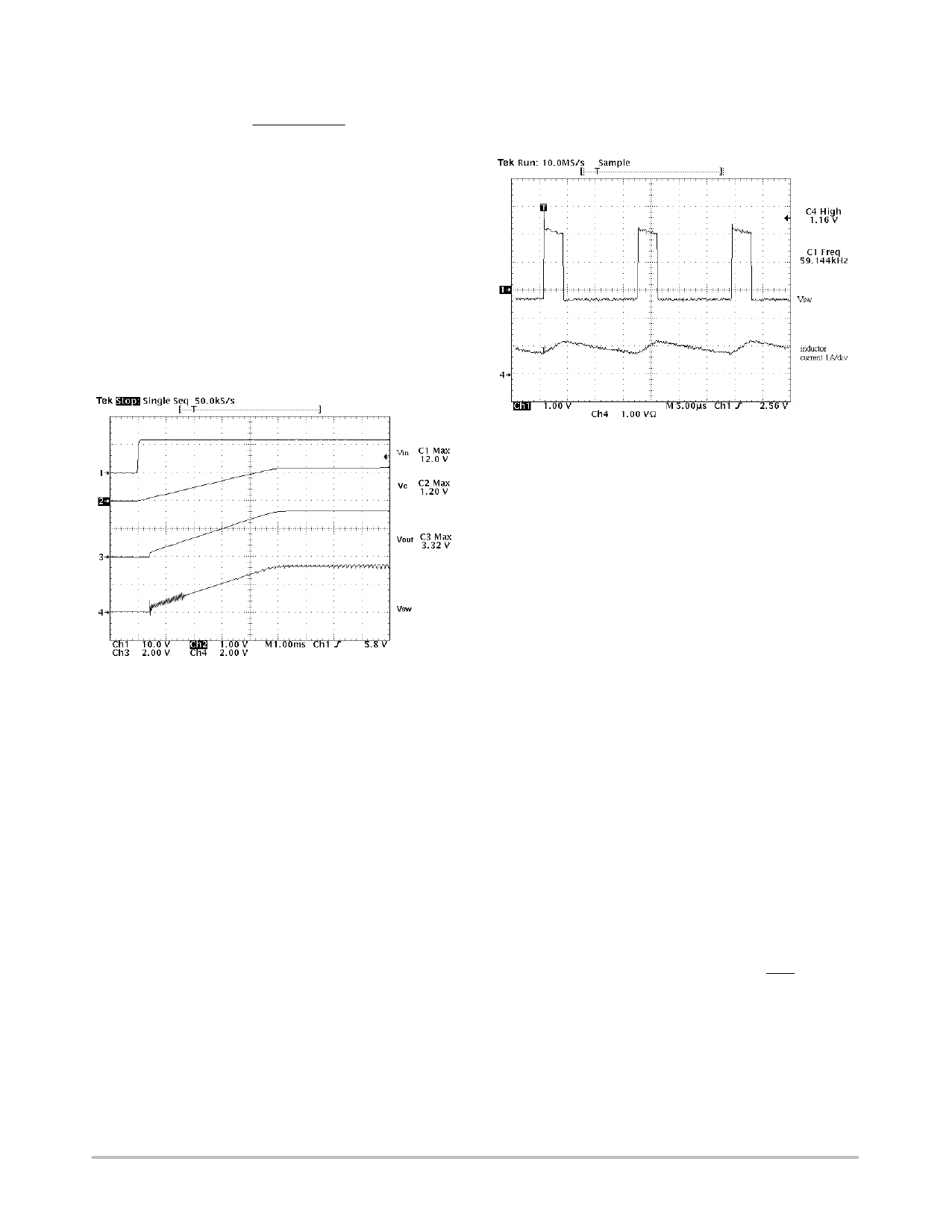
5.0 ms which is adequate to avoid any current stresses.
Figure 16 shows the gradual rise of the VC, VO and envelope
of the VSW during power up. There is no voltage overshoot
after the output voltage reaches the regulation. If the supply
voltage rises slower than the VC pin, output voltage may
overshoot.
Figure 15. SHDNB pin equivalent internal circuit (a)
and practical interface examples (b), (c).
Figure 15(a) depicts the SHDNB pin equivalent internal
circuit. If the pin is open, current source I1 flows into the
base of Q1, turning both Q1 and Q2 on. In turn, Q2 collector
current enables the various internal power rails. In
Figure 15(b), a standard logic gate is used to pull the pin low
by shunting I1 to ground, which places the IC in sleep
(shutdown) mode. Note that, when the gate output is logical
high, the voltage at the SHDNB pin will rise to the internal
clamp voltage of 8 V. This level exceeds the maximum
output rating for most common logic families. Protection
Zener diode Z1 permits the pin voltage to rise high enough
to enable the IC, but remain less than the gate output voltage
rating. In Figure 15(c), a single open-collector general-
purpose NPN transistor is used to pull the pin low. Since
transistors generally have a maximum collector voltage
rating in excess of 8 V, the protection Zener diode in
Figure 15(b) is not required.
Startup
During power up, the regulator tends to quickly charge up
the output capacitors to reach voltage regulation. This gives
rise to an excessive in−rush current which can be detrimental
to the inductor, IC and catch diode. In V2 control, the
compensation capacitor provides Soft−Start with no need
for extra pin or circuitry. During the power up, the Output
Source Current of the error amplifier charges the
compensation capacitor which forces VC pin and thus output
voltage ramp up gradually.
The Soft−Start duration can be calculated by
TSS
+
VC CCOMP
ISOURCE
Figure 16. The Power Up Transition of CS5141X
Regulator
Short Circuit
When the VFB pin voltage drops below Foldback
Threshold, the regulator reduces the peak current limit by
40% and switching frequency to 1/4 of the nominal
frequency. These features are designed to protect the IC and
external components during overload or short circuit
conditions. In those conditions, peak switching current is
clamped to the current limit threshold. The reduced
switching frequency significantly increases the ripple
current, and thus lowers the DC current. The short circuit can
cause the minimum duty cycle to be limited by Minimum
Output Pulse Width. The foldback frequency reduces the
minimum duty cycle by extending the switching cycle. This
protects the IC from overheating, and also limits the power
that can be transferred to the output. The current limit
foldback effectively reduces the current stress on the
inductor and diode. When the output is shorted, the DC
current of the inductor and diode can approach the current
limit threshold. Therefore, reducing the current limit by 40%
can result in an equal percentage drop of the inductor and
diode current. The short circuit waveforms are captured in
http://onsemi.com
11
Share Link: