C1210 데이터 시트보기 (PDF) - IMP, Inc
부품명
상세내역
일치하는 목록
C1210 Datasheet PDF : 4 Pages
| |||

Process C1210
Physical Characteristics
Starting Material
Starting Mat. Resistivity
Typ. Operating Voltage
Well Type
Metal Layers
Poly Layers
Contact Size
Via Size
Metal-1 Width/Space
Metal-2 Width/Space
Gate Poly Width/Space
EPI P <100>
7 - 8.5 Ω-cm
5V
N-well
2
2
1.5x1.5µm
1.5x1.5µm
2.5 / 1.5µm
2.5 / 1.5µm
1.5 / 2.0µm
N+/P+ Width/Space
N+ To P+ Space
Contact To Poly Space
Contact Overlap Of Diffusion
Contact Overlap Of Poly
Metal-1 Overlap Of Contact
Metal-1 Overlap Of Via
Metal-2 Overlap Of Via
Minimum Pad Opening
Minimum Pad-to-Pad Spacing
Minimum Pad Pitch
2.5/ 2.0µm
9.0µm
1.5µm
1.0µm
1.0µm
1.0µm
1.0µm
1.0µm
65x65µm
5.0µm
80.0µm
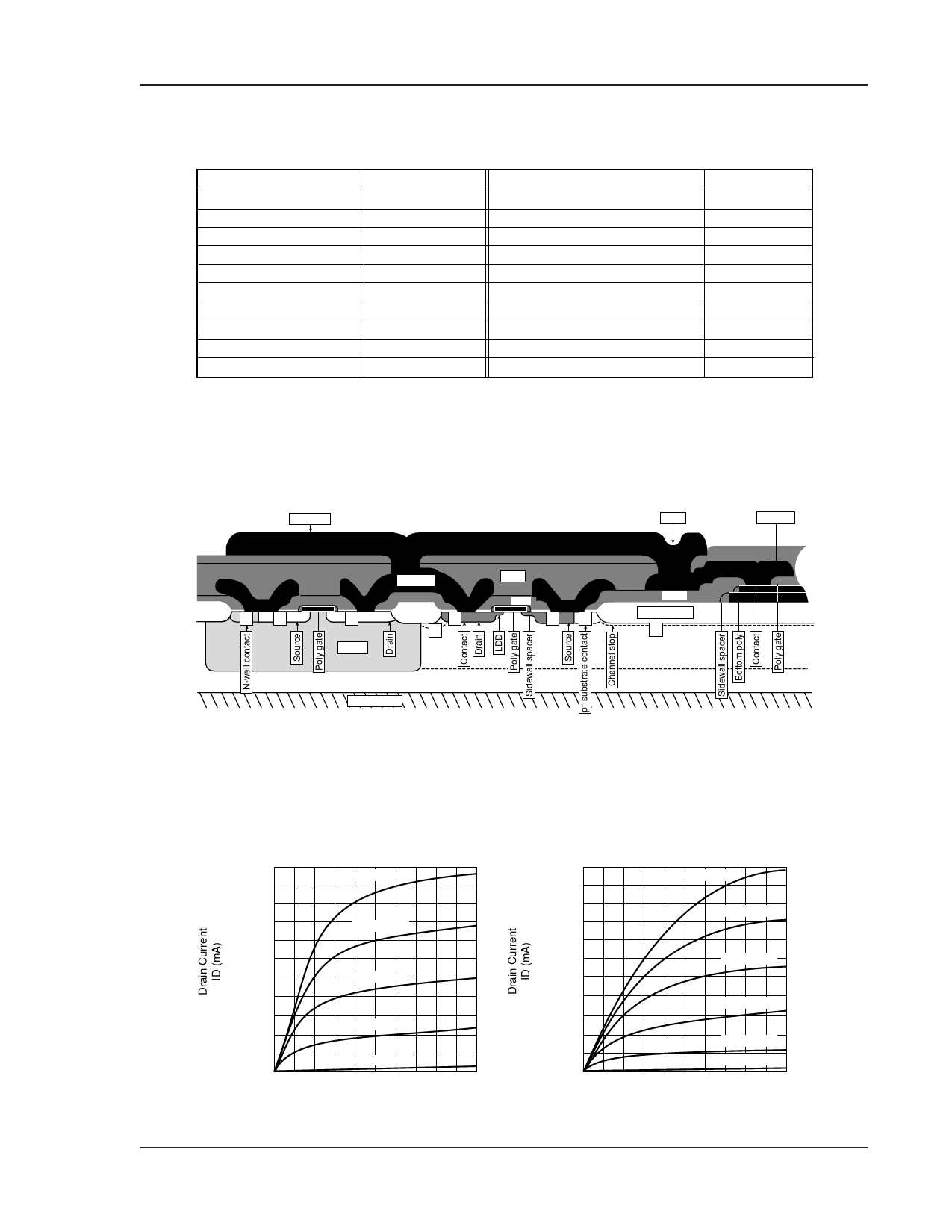
Special Feature of C1210 Process: This process offers zero threshold n- and p-channel
transistors in addition to normal threshold transistors of CMOS 1.2µm technology.
Metal 2
VIA
n+
p+
Metal 1
p+
N-well
n+
p
p+ substrate
p–epi
SIO2
LTO
n+
p+
LTO
Field Oxide
p
Cross-Sectional view of the LVMOS process
Metal 1
5.5
0.55 mA
/div
ID vs VD, W/L = 20/1.2
VGS = 4.0V
VGS = 3.0V
VGS = 2.0V
VGS = 1.0V
VGS = 0V
.00
0
1
2
3
4
5
Drain Voltage (v) VDS
n-ch Transistor IV characteristics of a 20/1.2 device
ID vs VD, W/L = 20/1.2
-3.0
VGS = –5.0V
VGS = –4.0V
0.3 mA
/div
VGS = –3.0V
VGS = –2.0V
VGS = –1.0V
VGS = 0.0V
.00
0 –1 –2 –3 – 4 –5
Drain Voltage (v) VDS
p-ch Transistor IV characteristics of a 20/1.2 device
© IMP, Inc.
49