BGA430(2001) 데이터 시트보기 (PDF) - Infineon Technologies
부품명
상세내역
일치하는 목록
BGA430 Datasheet PDF : 10 Pages
| |||
Preliminary
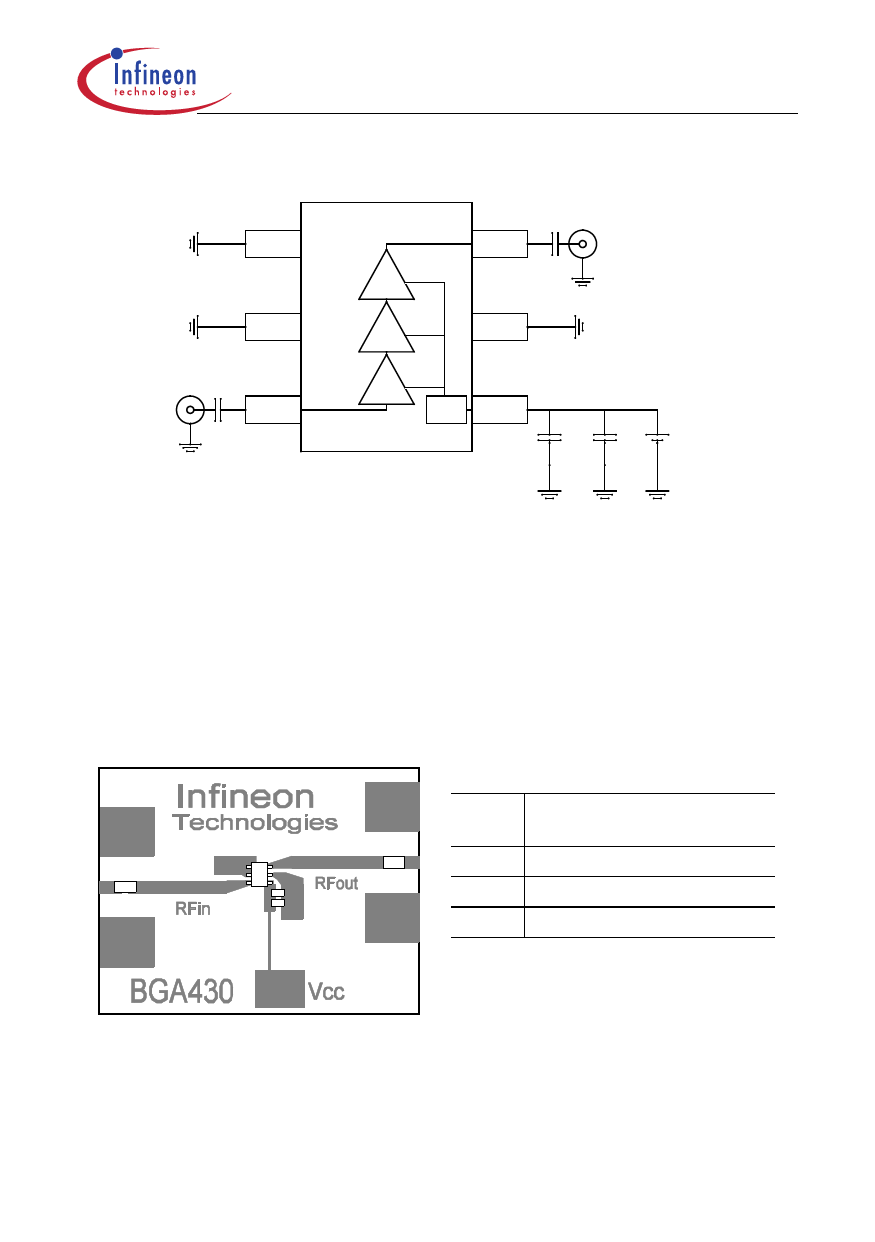
Typical Application
In,6
BGA430
Vcc, 1
C3 C4
Out, 3
Out
GND1, 5,2
GND2, 4
Fig. 1: Typical application circuit
Notes:
Due to the high gain of the BGA430 RF blocking at the supply pin (VCC) has to be done
very carefully. Abroad band low impedance RF path to GND has to be provided at VCC.
If no appropriate RF blocking is used, RF can couple via the internal power lines to the
input and the circuit may oscillate.
PCB - Layouts for the application circuit
BGA430
C1
in
IC1
C2
C3
C4
Vcc
Part list:
C1, C2 coupling capacitors
(not used for measurements)
C3
100pF
C4
100pF
IC1
BGA430
BGA430
in
PCB data: glass fiber epoxy board (double sided), 0.5mm, εr=4.8
Preliminary data sheet
8
Vcc
2001-04-24
Share Link: 