APX9266 데이터 시트보기 (PDF) - Anpec Electronics
부품명
상세내역
일치하는 목록
APX9266 Datasheet PDF : 14 Pages
| |||
APX9266
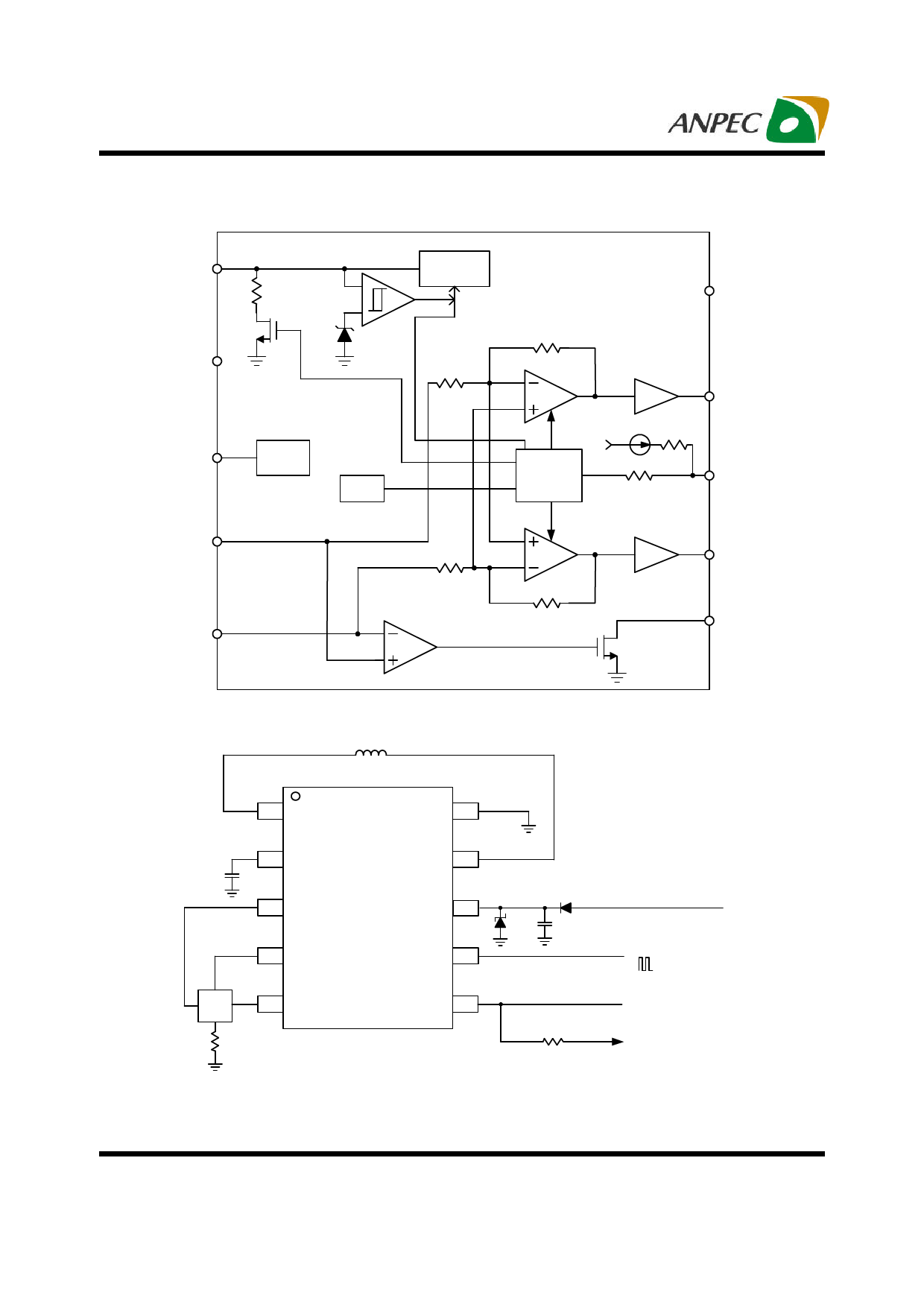
Block Diagram
CT
VCC
HB
IN+
IN-
Discharge
Circuit
GND
500Ω
Hall
Bias
TSD
150kΩ
3µA 90kΩ
Vcc
Control
10kΩ
OUT1
PWM
500Ω
150kΩ
OUT2
FG
Typical Application Circuit
CCT
0.47µF
1 OUT2
2 CT
3 IN+
4 HB
GND 10
OUT1 9
Zener
D1
VCC 8
VIN
D2
C1
PWM 7
6V 1µF
PWM control
signal
Hall
5 IN-
FG 6
RFG
10kΩ
FG output
Pull High
Voltage
Note 3: In hot plug application, it’s necessary to protect against a hot plug input voltage overshoot. Add an input zener diode, between
the VCC and GND, to clamp the overshoot. In normal operation, the zener diode isn’t stressed because output current
doesn’t reverse to VCC.
Copyright © ANPEC Electronics Corp.
7
Rev. A.4 - Mar., 2008
www.anpec.com.tw
Share Link: 