APX9266 데이터 시트보기 (PDF) - Anpec Electronics
부품명
상세내역
일치하는 목록
APX9266 Datasheet PDF : 14 Pages
| |||
APX9266
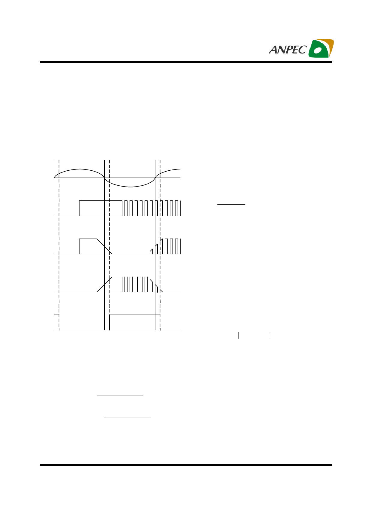
Application Information (Cont.)
PWM input (Cont.)
The input level of PWM terminal is
H : High side output transistor is ON
L : High side output transistor is OFF
(see Truth Table).
When PWM terminal is open, it is equal to high
IN+
PWM
OUT1
OUT2
FG
Figure 4.PWM Input Waveform
CT Capacitor
The capacitor that is connected from CT pin to GND
determines the shutdown time and restart time.
( ) Restart Time = CCT × VCTH − VCTL
ICT1
( ) Shutdown Time = CCT × VCTH − VCTL
ICT2
Where:
CCT = CT pin capacitor
For example:
CCT= 0.47µF
Restart Time=0.52s, Shutdown Time=3.13s
The value of charge capacitor in range of 0.47µF to 1µF
is recommended .
FG Resistor
The value of the FG resistor could be decided by the fol-
lowing equation:
V V RFG =
CC − FG
I
For example:
VCC= 5V, I=3mA, VFG= 0.2V, RFG= 1.6kΩ
The value of resistor in the range of 1KΩ to 10KΩ is
recommended.
Thermal Consideration
Refer to “Maximum Power Dissipation vs. Ambient
Temperature”, the IC is safe to operate below the curve
and it will eable the thermal protection if the operating
area is above the line. For example, TA= 75°C, the
maximum power dissipation is about 0.48w.
The power dissipation can be calculated by the following
equation:
PD = (VCC − VOUT1−VOUT2 ) × IOUT + VCC × ICC
For example:
if VCC=5V, ICC=4mA, IOUT=300mA, VOUT1=4.81V,
V =0.17V, then P =0.128W
OUT2
D
The GND pin provides an electrical connection to ground
and channeling heat away. The printed circuit board (PCB)
forms a heat sink and dissipates most of the heat into
ambient air.
Copyright © ANPEC Electronics Corp.
10
Rev. A.4 - Mar., 2008
www.anpec.com.tw
Share Link: 