APX9131(2009) 데이터 시트보기 (PDF) - Anpec Electronics
부품명
상세내역
일치하는 목록
APX9131 Datasheet PDF : 14 Pages
| |||
APX9131
Operating Waveforms
Output Switch Waveform
Output Switch Waveform
VDD=3V
RL=5.1kΩ
CL=12pF
VOUT=0.5V/div
Time (50µs/div)
VDD=3V
RL=5.1kΩ
CL=12pF
VOUT=0.5V/div
0
Time (2µs/div)
Pin Description
PIN
NO.
NAME
1
VDD
2
VOUT
3
GND
FUNCTION
Power Input
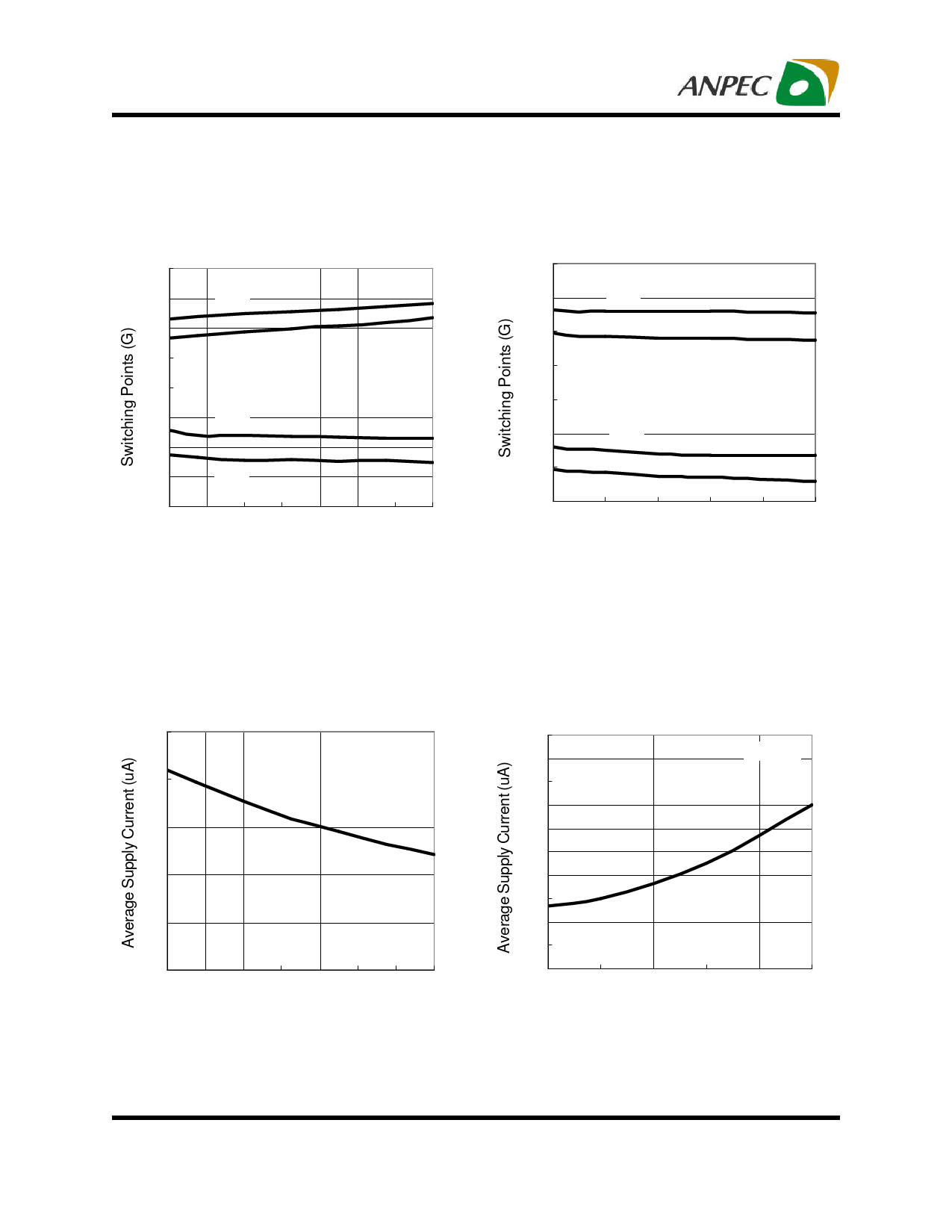
When a magnetic field enters the hall element and exceeds the operate point BOPS (or less than
BOPN), the output turns on (output is low). When the magnetic field is below the release point BRPS
(or above BRPN), the output turns off (output is high). It is designed with open drain configuration
and connecting a pull up resistor from VOUT to VDD is necessary. It cannot be floating.
Ground Connection.
Copyright © ANPEC Electronics Corp.
4
Rev. A.12 - Aug., 2009
www.anpec.com.tw
Share Link: 