7411(2017) 데이터 시트보기 (PDF) - Analog Devices
부품명
상세내역
일치하는 목록
7411
(Rev.:2017)
(Rev.:2017)
Analog Devices

7411 Datasheet PDF : 36 Pages
| |||
ADT7411
Data Sheet
FUNCTIONAL DESCRIPTION
ANALOG INPUTS
INT VREF
VDD
Single-Ended Inputs
The ADT7411 offers eight single-ended analog input channels.
The analog input range is from 0 V to 2.25 V or 0 V to VDD. To
maintain the linearity specification, it is recommended that the
maximum VDD value be set at 5 V. Selection between the two
input ranges is done by Bit C4 of the Control Configuration 3
register (Address 1Ah). Setting this bit to 0 sets up the analog
input ADC reference to be sourced from the internal voltage
reference of 2.25 V. Setting the bit to 1 sets up the ADC
reference to be sourced from VDD.
The ADC resolution is 10 bits and is mostly suitable for dc
input signals or very slowly varying ac signals. Bit C1 and
Bit C2 of the Control Configuration 1 register (Address 18h) are
used to set up Pin 7 and Pin 8 as AIN1 and AIN2. Figure 20
shows the overall view of the 8-channel analog input path.
AIN1
M
AIN2
U
AIN3
L
T
AIN4
I
AIN5
P
L
AIN6
E
X
AIN7
E
AIN8
R
10-BIT
ADC
TO ADC
VALUE
REGISTER
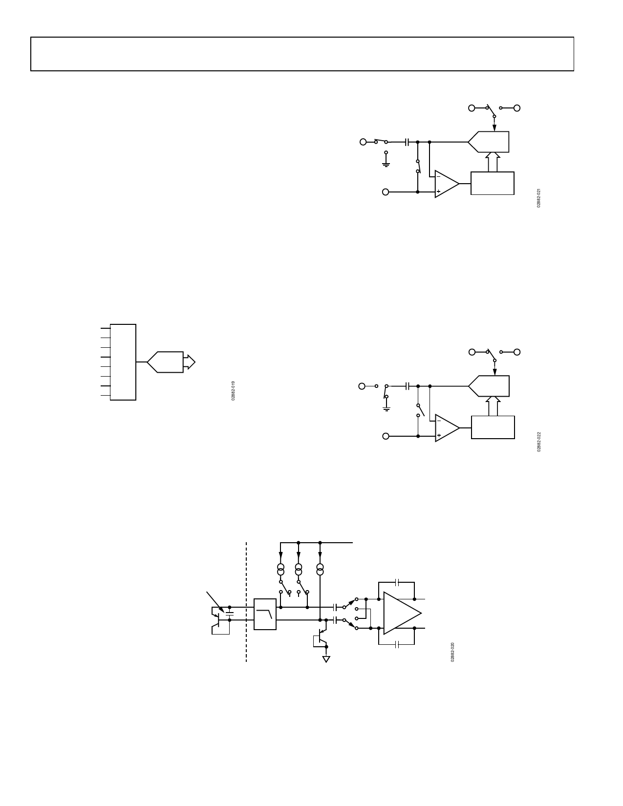
Figure 20. Octal Analog Input Path
SAMPLING
REF
A CAPACITOR
AIN
CAP DAC
SW1 B
ACQUISITION
SW2
PHASE
REF/2
COMPARATOR
CONTROL
LOGIC
Figure 21. ADC Acquisition Phase
When the ADC eventually goes into conversion phase (see
Figure 22) SW2 opens and SW1 moves to Position B, causing
the comparator to become unbalanced. The control logic and
the DAC are used to add and subtract fixed amounts of charge
from the sampling capacitor to bring the comparator back into
a balanced condition. When the comparator is rebalanced, the
conversion is complete. The control logic generates the ADC
output code. Figure 24 shows the ADC transfer function for
single-ended analog inputs.
INT VREF
VDD
SAMPLING
REF
A CAPACITOR
AIN
CAP DAC
SW1 B
CONVERSION
SW2
PHASE
Converter Operation
The analog input channels use a successive approximation ADC
based around a capacitor DAC. Figure 21 and Figure 22 show
simplified schematics of the ADC. Figure 21 shows the ADC
during acquisition phase. SW2 is closed and SW1 is in Position A.
The comparator is held in a balanced condition and the
sampling capacitor acquires the signal on AIN.
REF/2
COMPARATOR
CONTROL
LOGIC
Figure 22. ADC Conversion Phase
VDD
OPTIONAL CAPACITOR, UP TO
3nF MAX. CAN BE ADDED TO
IMPROVE HIGH FREQUENCY
NOISE REJECTION IN NOISY
ENVIRONMENTS
I
N × I IBIAS
REMOTE
SENSING
TRANSISTOR
(2N3906)
D+
C1
D–
LOW-PASS
FILTER
fC = 65kHz
BIAS
DIODE
VOUT+
TO ADC
VOUT–
Figure 23. Signal Conditioning for External Diode Temperature Sensor
Rev. C | Page 14 of 36
Share Link: