ADG508FBNZ 데이터 시트보기 (PDF) - Analog Devices
부품명
상세내역
일치하는 목록
ADG508FBNZ Datasheet PDF : 20 Pages
| |||
ADG508F/ADG509F
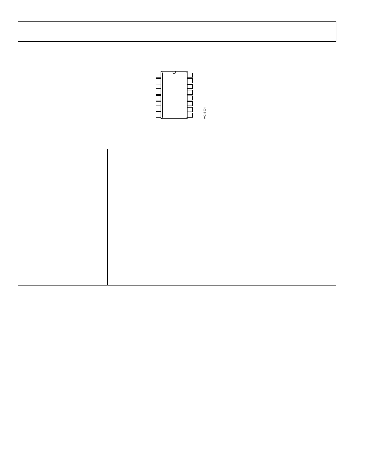
PIN CONFIGURATION AND FUNCTION DESCRIPTIONS
A0 1
16 A1
EN 2
15 A2
VSS 3 ADG508F 14 GND
S1 4 TOP VIEW 13 VDD
S2 5 (Not to Scale) 12 S5
S3 6
11 S6
S4 7
10 S7
D8
9 S8
Figure 3. ADG508F Pin Configuration
Table 5. ADG508F Pin Function Descriptions
Pin No.
Mnemonic
Description
1
A0
Logic Control Input.
2
EN
Active High Digital Input. When low, the device is disabled and all switches are off. When high,
Ax logic inputs determine on switches.
3
VSS
Most Negative Power Supply Potential. In single-supply applications, this pin can be connected
to ground.
4
S1
Source Terminal 1. This pin can be an input or an output.
5
S2
Source Terminal 2. This pin can be an input or an output.
6
S3
Source Terminal 3. This pin can be an input or an output.
7
S4
Source Terminal 4. This pin can be an input or an output.
8
D
Drain Terminal. This pin can be an input or an output.
9
S8
Source Terminal 8. This pin can be an input or an output.
10
S7
Source Terminal 7. This pin can be an input or an output.
11
S6
Source Terminal 6. This pin can be an input or an output.
12
S5
Source Terminal 5. This pin can be an input or an output.
13
VDD
Most Positive Power Supply Potential.
14
GND
Ground (0 V) Reference.
15
A2
Logic Control Input.
16
A1
Logic Control Input.
Rev. F | Page 6 of 20
Share Link: 