AD9444 데이터 시트보기 (PDF) - Analog Devices
부품명
상세내역
일치하는 목록
AD9444 Datasheet PDF : 40 Pages
| |||
AD9444
SWITCHING SPECIFICATIONS
AVDD1 = 3.3 V, AVDD2 = 5.0 V, DRVDD = 3.3 V, unless otherwise noted.
Table 4.
Parameter
CLOCK INPUT PARAMETERS
Maximum Conversion Rate
Minimum Conversion Rate
CLK Period
CLK Pulse Width High1 (tCLKH)
CLK Pulse Width Low1 (tCLKL)
DATA OUTPUT PARAMETERS
Output Propagation Delay—CMOS (tPD)2 (DX, DCO+)
Output Propagation Delay—LVDS (tPD)3 (DX+, DCO+)
Pipeline Delay (Latency)
Aperture Delay (tA)
Aperture Uncertainty (Jitter, tJ)
Temp
Full
Full
Full
Full
Full
Full
Full
Full
Full
Full
Test Level
VI
V
V
V
V
IV
VI
V
V
V
AD9444BSVZ-80
Min Typ Max Unit
80
MSPS
10
MSPS
12.5
ns
4
ns
4
ns
3
5.25 8
ns
3
5
7.5
ns
12
Cycles
ns
0.2
ps rms
1 With duty cycle stabilizer (DCS) enabled.
2 Output propagation delay is measured from clock 50% transition to data 50% transition, with 5 pF load.
3 LVDS RTERM = 100 Ω. Measured from the 50% point of the rising edge of CLK+ to the 50% point of the data transition.
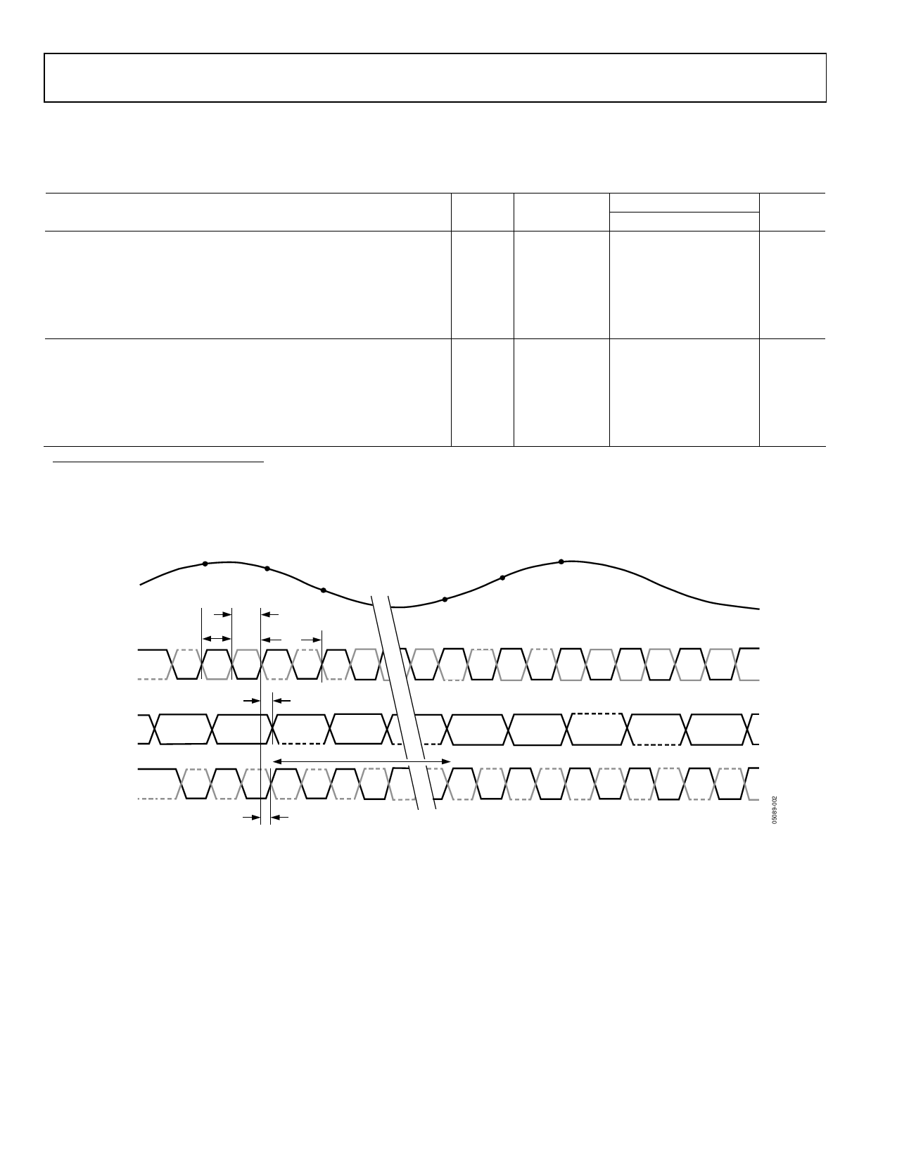
AIN
CLK+
CLK–
DATA OUT
DCO+
DCO–
N–1
N
N+1
tCLKL
tCLKH
1/fS
tPD
N–12
N–11
12 CLOCK CYCLES
N
N+1
tCPD
Figure 2. LVDS Mode Timing Diagram
Rev. 0 | Page 6 of 40
Share Link: 