74LVC594A(2017) 데이터 시트보기 (PDF) - NXP Semiconductors.
부품명
상세내역
일치하는 목록
74LVC594A Datasheet PDF : 21 Pages
| |||
Nexperia
74LVC594A
8-bit shift register with output register
Symbol Parameter
Conditions
trec
fmax
tsk(o)
CPD
recovery time
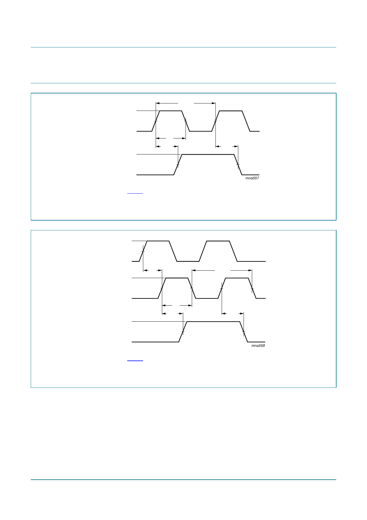
SHR to SHCP, STR to STCP;
see Figure 11 and Figure 12
VCC = 1.65 V to 1.95 V
VCC = 2.3 V to 2.7 V
VCC = 2.7 V
VCC = 3.0 V to 3.6 V
maximum
frequency
SHCP or STCP; see Figure 7
and Figure 8
VCC = 1.65 V to 1.95 V
output skew time
VCC = 2.3 V to 2.7 V
VCC = 2.7 V
VCC = 3.0 V to 3.6 V
VCC = 3.0 V to 3.6 V
power dissipation
capacitance
VI = GND to VCC
VCC = 1.65 V to 1.95 V
VCC = 2.3 V to 2.7 V
VCC = 3.0 V to 3.6 V
-40 °C to +85 °C -40 °C to +125 °C Unit
Min Typ[1] Max
Min
Max
5.0 -2.7
-
5.5
4.0 -1.5
-
4.5
2.0 -1.0
-
2.5
2.0 -1.0
-
2.5
-
ns
-
ns
-
ns
-
ns
80
130
-
70
100 140
-
90
110 150
-
100
130 180
-
115
[4]
-
-
1.0
-
[5]
-
50
-
-
-
45
-
-
-
44
-
-
-
MHz
-
MHz
-
MHz
-
MHz
1.5 ns
-
pF
-
pF
-
pF
[1] Typical values are measured at Tamb = 25 °C and VCC = 1.8 V, 2.5 V, 2.7 V, and 3.3 V respectively.
[2] tpd is the same as tPLH and tPHL.
[3] Cascadability is guaranteed under identical VCC and temperature conditions.
[4] Skew between any two outputs of the same package switching in the same direction. This parameter is guaranteed by design.
[5] CPD is used to determine the dynamic power dissipation (PD in μW).
PD = CPD x VCC2 x fi x N + ∑(CL x VCC2 x fo) where:
fi = input frequency in MHz;
fo = output frequency in MHz;
CL = output load capacitance in pF;
VCC = supply voltage in V;
N = number of inputs switching;
∑(CL x VCC2 x fo) = sum of outputs.
74LVC594A
Product data sheet
All information provided in this document is subject to legal disclaimers.
Rev. 3 — 20 July 2017
© Nexperia B.V. 2017. All rights reserved.
10 / 21
Share Link: 