74LV595 데이터 시트보기 (PDF) - Philips Electronics
부품명
상세내역
일치하는 목록
74LV595
Philips Electronics

74LV595 Datasheet PDF : 16 Pages
| |||
Philips Semiconductors
8-bit serial-in/serial or parallel-out shift register
with output latches (3-State)
Product specification
74LV595
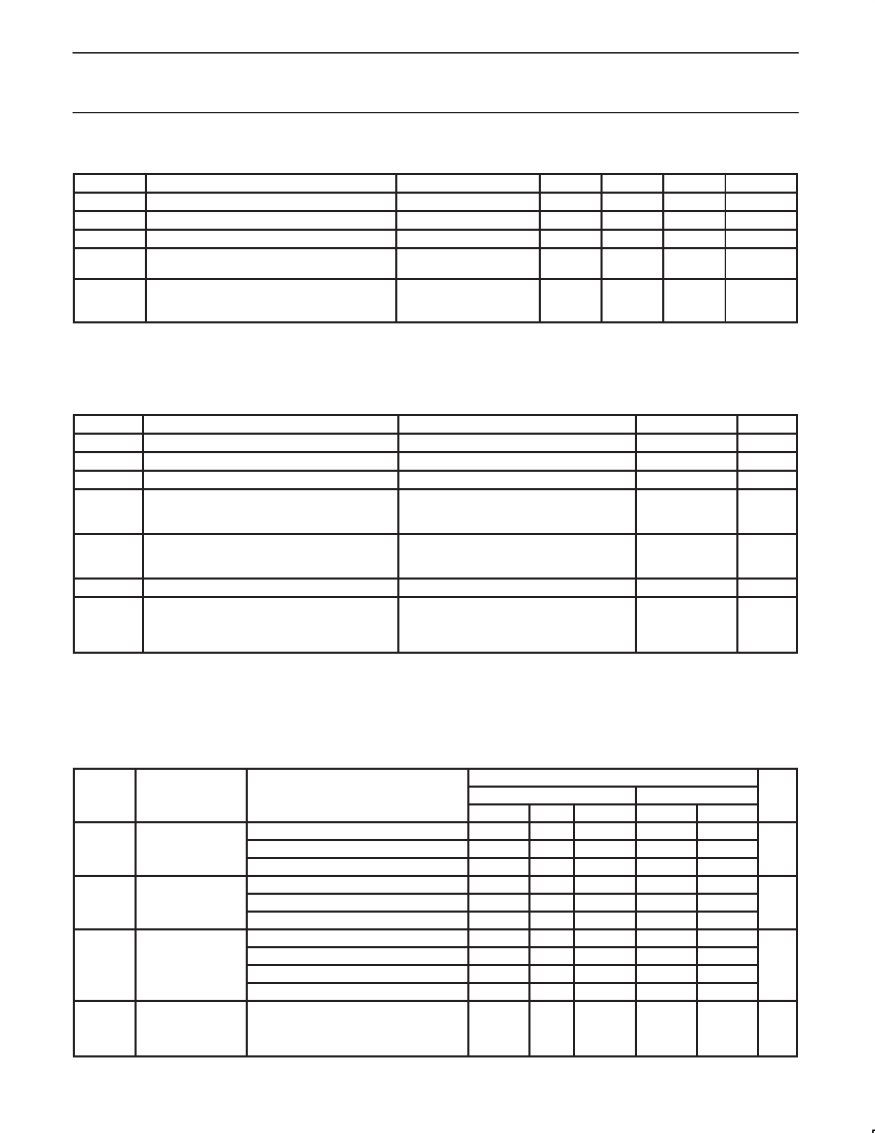
RECOMMENDED OPERATING CONDITIONS
SYMBOL
PARAMETER
CONDITIONS
MIN
TYP.
MAX
UNIT
VCC
VI
VO
Tamb
DC supply voltage
Input voltage
Output voltage
Operating ambient temperature range in free
air
See Note1
See DC and AC
characteristics
1.0
3.3
3.6
V
0
–
VCC
V
0
–
VCC
V
–40
–40
+85
+125
°C
tr, tf
Input rise and fall times
VCC = 1.0V to 2.0V
–
VCC = 2.0V to 2.7V
–
VCC = 2.7V to 3.6V
–
–
500
–
200
ns/V
–
100
NOTE:
1. The LV is guaranteed to function down to VCC = 1.0V (input levels GND or VCC); DC characteristics are guaranteed from VCC = 1.2V to VCC =3.6V.
ABSOLUTE MAXIMUM RATINGS1, 2
In accordance with the Absolute Maximum Rating System (IEC 134)
Voltages are referenced to GND (ground = 0V)
SYMBOL
PARAMETER
CONDITIONS
RATING
UNIT
VCC
±IIK
±IOK
±IO
DC supply voltage
DC input diode current
DC output diode current
DC output source or sink current
– standard outputs
– bus driver outputs
VI < –0.5 or VI > VCC + 0.5V
VO < –0.5 or VO > VCC + 0.5V
–0.5V < VO < VCC + 0.5V
–0.5 to +4.6
V
20
mA
50
mA
25
mA
35
±IGND,
±ICC
DC VCC or GND current for types with
–standard outputs
–bus driver outputs
50
mA
70
Tstg
Storage temperature range
–65 to +150
°C
Power dissipation per package
for temperature range: –40 to +125°C
PTOT
–plastic DIL
–plastic mini-pack (SO)
above +70°C derate linearly with 12mW/K
above +70°C derate linearly with 8 mW/K
750
500
mW
–plastic shrink mini-pack (SSOP and TSSOP) above +60°C derate linearly with 5.5 mW/K
400
NOTES:
1. Stresses beyond those listed may cause permanent damage to the device. These are stress ratings only and functional operation of the
device at these or any other conditions beyond those indicated under “recommended operating conditions” is not implied. Exposure to
absolute-maximum-rated conditions for extended periods may affect device reliability.
2. The input and output voltage ratings may be exceeded if the input and output current ratings are observed.
DC CHARACTERISTICS
Over recommended operating conditions voltages are referenced to GND (ground = 0V)
LIMITS
SYMBOL PARAMETER
TEST CONDITIONS
-40°C to +85°C
MIN
TYP1 MAX
VCC = 1.2V
0.9
VIH
HIGH level Input
voltage
VCC = 2.0V
1.4
VCC = 2.7 to 3.6V
2.0
VCC = 1.2V
0.3
VIL
LOW level Input
voltage
VCC = 2.0V
0.6
VCC = 2.7 to 3.6V
0.8
VCC = 1.2V; VI = VIH or VIL; –IO = 100µA
1.2
VOH
HIGH level output VCC = 2.0V; VI = VIH or VIL; –IO = 100µA
voltage; all outputs VCC = 2.7V; VI = VIH or VIL; –IO = 100µA
1.8
2.5
2.0
2.7
VCC = 3.0V; VI = VIH or VIL; –IO = 100µA
2.8
3.0
HIGH level output
VOH
voltage;
STANDARD
VCC = 3.0V;VI = VIH or VIL; –IO = 6mA
outputs
2.40
2.82
-40°C to +125°C
MIN
MAX
0.9
1.4
2.0
0.3
0.6
0.8
1.8
2.5
2.8
2.20
UNIT
V
V
V
V
1998 Apr 20
6
Share Link: