74LV573 데이터 시트보기 (PDF) - Philips Electronics
부품명
상세내역
일치하는 목록
74LV573 Datasheet PDF : 14 Pages
| |||
Philips Semiconductors
Octal D-type transparent latch (3-State)
Product specification
74LV573
FEATURES
• Wide operating voltage: 1.0 to 5.5V
• Optimized for Low Voltage applications: 1.0V to 3.6V
• Accepts TTL input levels between VCC = 2.7V and VCC = 3.6V
• Typical VOLP (output ground bounce) < 0.8V at VCC = 3.3V,
Tamb = 25°C
• Typical VOHV (output VOH undershoot) > 2V at VCC = 3.3V,
Tamb = 25°C
• Inputs and outputs on opposite sides of package allowing easy
interface with microprocessors
• Useful as input or output port for microprocessors/microcomputer
• Common 3-State output enable input
• Output capability: bus driver
• ICC category: MSI
DESCRIPTION
The 74LV573 is a low-voltage Si-gate CMOS device that is pin and
function compatible with 74HC/HCT573.
The 74LV573 is an octal D-type transparent latch featuring separate
D-type inputs for each latch and 3-State outputs for bus oriented
applications. A latch enable (LE) input and an output enable (OE)
input are common to all internal latches.
The ‘573’ consists of eight D-type transparent latches with 3-State
true outputs. When LE is HIGH, data at the Dn inputs enters the
latches. In this condition the latches are transparent, i.e., a latch
output will change each time its corresponding D-input changes.
When LE is LOW the latches store the information that was present
at the D-inputs a set-up time preceding the HIGH-to-LOW transition
of LE. When OE is LOW, the contents of the eight latches are
available at the outputs. When OE is HIGH, the outputs go to the
high impedance OFF-state. Operation of the OE input does not
affect the state of the latches.
The ‘573’ is functionally identical to the ‘563’ and the ‘373’, but the
‘563’ has inverted outputs and the ‘373’ has a different pin
arrangement.
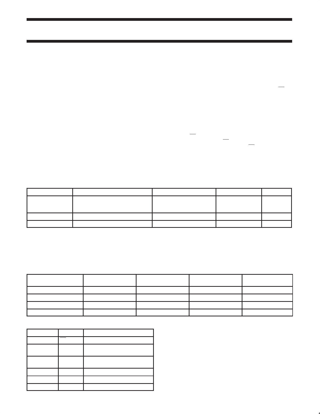
QUICK REFERENCE DATA
GND = 0V; Tamb = 25°C; tr = tf v2.5 ns
SYMBOL
PARAMETER
CONDITIONS
tPHL/tPLH
Propagation delay
Dn to Qn
LE to Qn
CL = 15pF
VCC = 3.3V
CI
Input capacitance
CPD
Power dissipation capacitance per latch Notes 1, 2
NOTES:
1. CPD is used to determine the dynamic power dissipation (PD in µW)
PD = CPD VCC2 x fi )ȍ (CL VCC2 fo) where:
fi = input frequency in MHz; CL = output load capacity in pF;
fo = output frequency in MHz; VCC = supply voltage in V;
ȍ (CL VCC2 fo) = sum of the outputs.
2. The condition is VI = GND to VCC.
TYPICAL
12
13
3.5
26
UNIT
ns
pF
pF
ORDERING AND PACKAGE INFORMATION
PACKAGES
TEMPERATURE RANGE
20-Pin Plastic DIL
20-Pin Plastic SO
20-Pin Plastic SSOP Type II
20-Pin Plastic TSSOP Type I
–40°C to +125°C
–40°C to +125°C
–40°C to +125°C
–40°C to +125°C
OUTSIDE NORTH
AMERICA
74LV573 N
74LV573 D
74LV573 DB
74LV573 PW
NORTH AMERICA
74LV573 N
74LV573 D
74LV573 DB
74LV573PW DH
PKG. DWG. #
SOT146-1
SOT163-1
SOT339-1
SOT360-1
PIN DESCRIPTION
PIN NUMBER SYMBOL
1
OE
2, 3, 4, 5,
6, 7, 8, 9
D0–D7
19, 18, 17, 16,
15, 14, 13, 12
Q0–Q7
10
GND
11
LE
20
VCC
FUNCTION
Output enabled input (active LOW)
Data inputs
Data outputs
Ground (0V)
Latch enable input (active HIGH)
Positive supply voltage
1998 Jun 10
2
853-1989 19545
Share Link: 