G913 데이터 시트보기 (PDF) - Global Mixed-mode Technology Inc
부품명
상세내역
일치하는 목록
G913 Datasheet PDF : 10 Pages
| |||

Global Mixed-mode Technology Inc.
G913
IN
OUT
+
R1
G913
SET
- BATTERY CIN
SHDN
1µF
GND
R2
OUTPUT
VOLTAGE
COUT RL
1µF
Where (TJ–TA) is the temperature difference the G913 die
and the ambient air,θJA, is the thermal resistance of the
chosen package to the ambient air. For surface mount
device, heat sinking is accomplished by using the heat
spreading capabilities of the PC board and its copper
traces. In the case of a SOT23-5 package, the thermal
resistance is typically 240oC/Watt. (See Recommended
Minimum Footprint) [Figure 3] Refer to Figure 4 is the
G913 valid operating region (Safe Operating Area) & refer
to Figure 5 is maximum power dissipation of SOT 23-5.
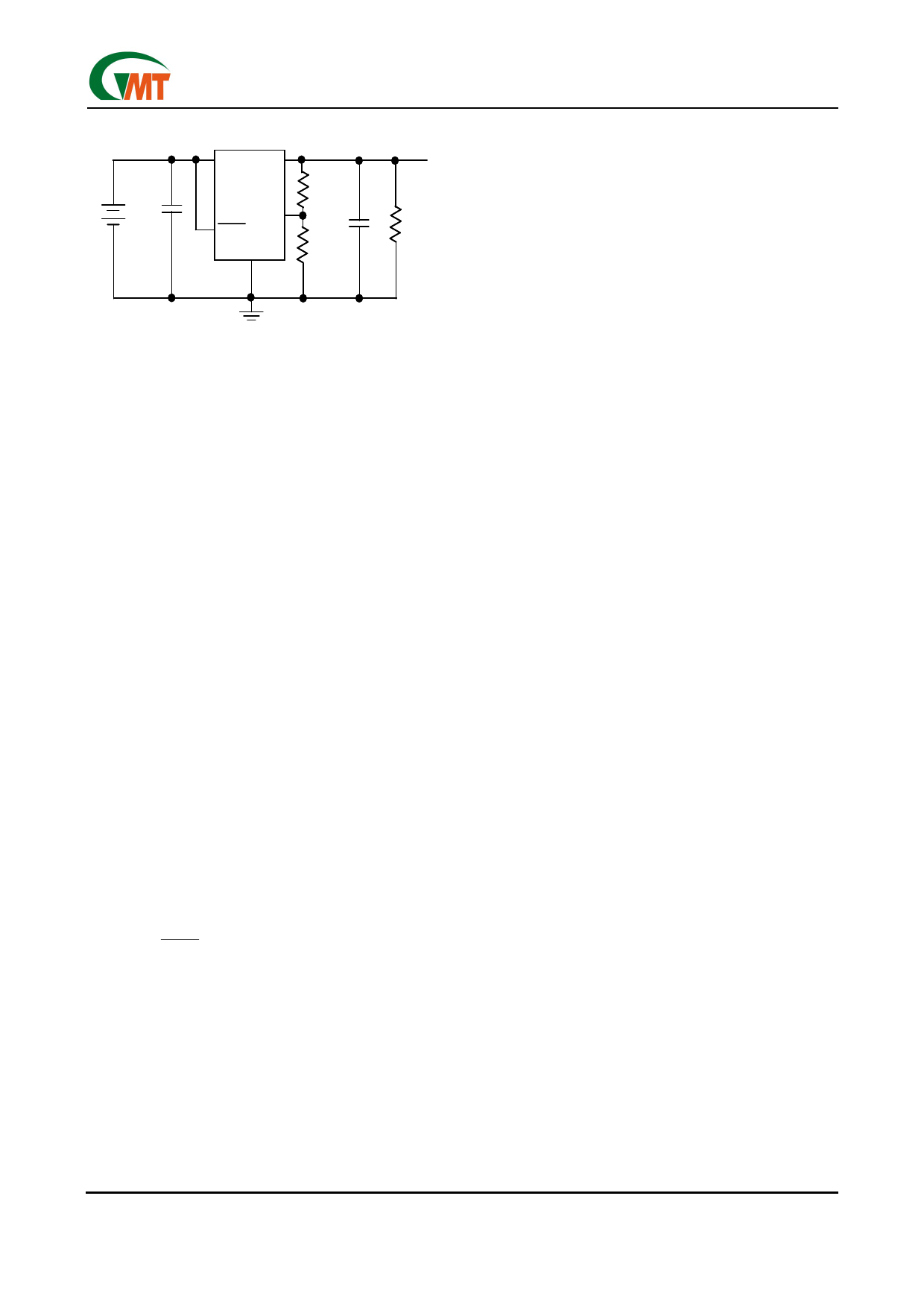
Figure 2. Adjustable Output Using External
Feedback Resistors
Over Current Protection
The G913 use a current mirror to monitor the output cur-
rent. A small portion of the PMOS output transistor’s cur-
rent is mirrored onto a resistor such that the voltage
across this resistor is proportional to the output current.
This voltage is compared against the 1.25V reference.
Once the output current exceeds the limit, the PMOS
output transistor is turned off. Once the output transistor is
turned off, the current monitoring voltage decreases to
zero, and the output PMOS is turned on again. If the over
current condition persist, the over current protection circuit
will be triggered again. Thus, when the output is shorted
to ground, the output current will be alternating between 0
and the over current limit. The typical over current limit of
the G913 is set to 250mA. Note that the input bypass
capacitor of 1µF must be used in this case to filter out the
input voltage spike caused by the surge current due to the
inductive effect of the package pin and the printed circuit
board’s routing wire. Otherwise, the actual voltage at the
IN pin may exceed the absolute maximum rating.
Over Temperature Protection
To prevent abnormal temperature from occurring, the
G913 has a built-in temperature monitoring circuit. When
it detects the temperature is above 150oC, the output
transistor is turned off. When the IC is cooled down to
below 135oC, the output is turned on again. In this way,
the G913 will be protected against abnormal junction
temperature during operation.
Shutdown Mode
When the SHDN pin is connected a logic low voltage,
the G913 enters shutdown mode. All the analog circuits
are turned off completely, which reduces the current
consumption to only the leakage current. The output is
disconnected from the input. When the output has no
load at all, the output voltage will be discharged to ground
through the internal resistor voltage divider.
Operating Region and Power Dissipation
Since the G913 is a linear regulator, its power dissipation
is always given by P = IOUT (VIN – VOUT). The maximum
power dissipation is given by:
PD(MAX) = (TJ–TA)/θJA,=150oC-25oC/240oC/W= 520mW
The die attachment area of the G913’s lead frame is
connected to pin 2, which is the GND pin. Therefore, the
GND pin of G913 can carry away the heat of the G913
die very effectively. To improve the power dissipation,
connect the GND pin to ground using a large ground
plane near the GND pin.
Applications Information
Capacitor Selection and Regulator Stability
Normally, use a 1µF capacitor on the input and a 1µF
capacitor on the output of the G913. Larger input capaci-
tor values and lower ESR provide better supply-noise
rejection and transient response. A higher- value input
capacitor (10µF) may be necessary if large, fast tran-
sients are anticipated and the device is located several
inches from the power source.
Power-Supply Rejection and Operation from Sources
Other than Batteries
The G913 is designed to deliver low dropout voltages and
low quiescent currents in battery powered systems.
Power-supply rejection is 42dB at low frequencies. As the
frequency increases above 20kHz, the output capacitor is
the major contributor to the rejection of power-supply
noise.
When operating from sources other than batteries, im-
prove supply-noise rejection and transient response by
increasing the values of the input and output capacitors,
and using passive filtering techniques.
Load Transient Considerations
The G913 load-transient response graphs show two
components of the output response: a DC shift of the
output voltage due to the different load currents, and the
transient response. Typical overshoot for step changes in
the load current from 0mA to 100mA is 12mV. Increasing
the output capacitor's value and decreasing its ESR at-
tenuates transient spikes.
Input-Output (Dropout) Voltage
A regulator's minimum input-output voltage differential (or
dropout voltage) determines the lowest usable supply
voltage. In battery-powered systems, this will determine
the useful end-of-life battery voltage. Because the G913
use a P-channel MOSFET pass transistor, their dropout
voltage is a function of RDS(ON) multiplied by the load cur-
rent.
Ver 0.9 Preliminary
Jan 25, 2002
TEL: 886-3-5788833
http://www.gmt.com.tw
8