G913 데이터 시트보기 (PDF) - Global Mixed-mode Technology Inc
부품명
상세내역
일치하는 목록
G913 Datasheet PDF : 10 Pages
| |||
Global Mixed-mode Technology Inc.
G913
Pin Description
PIN NAME
FUNCTION
1
Active-Low Shutdown Input. A logic low reduces the supply current to less than 1µA. Connect to IN for normal
SHDN
operation.
Ground. This pin also functions as a heatsink. Solder to large pads or the circuit board ground plane to
2
GND
maximize thermal dissipation.
3
IN
Regulator Input. Supply voltage can range from +2.5V to +5.5V. Bypass with 1µF to GND
Regulator Output. Fixed or adjustable from 1.25V to +5.5V. Sources up to 150mA. Bypass with a 1µF,
4
OUT <0.2Ω typical ESR capacitor to GND.
Feedback Input for Setting the Output Voltage. Connect to GND to set the output voltage to the preset
5
SET
2.84V or 3.15V or 3.30V or 3.00V. Connect to an external resistor divider for adjustable-output operation.
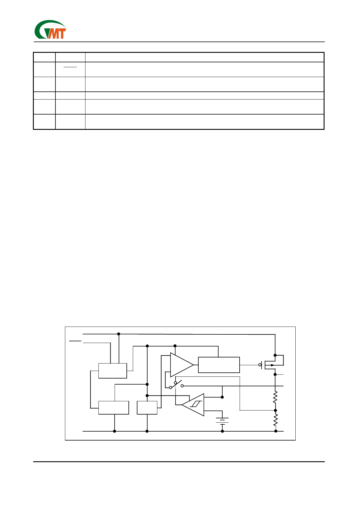
Detailed Description
The block diagram of the G913 is shown in Figure 1. It
consists of an error amplifier, 1.25V bandgap refer-
ence, PMOS output transistor, internal feedback volt-
age divider, mode comparator, shutdown logic, over
current protection circuit, and over temperature protec-
tion circuit.
The mode comparator compares the SET pin voltage
with an internal 120mV reference. If the SET pin volt-
age is less than 120mV, the internal feedback voltage
divider’s central tap is connected to the non-inverting
input of the error amplifier. The error amplifier com-
pares non-inverting input with the 1.25V bandgap ref-
erence. If the feedback voltage is higher than 1.25V,
the error amplifier’s output becomes higher so that the
PMOS output transistor has a smaller gate-to-source
voltage (VGS). This reduces the current carrying capa-
bility of the PMOS output transistor, as a result the
output voltage decreases until the feedback voltage is
equal to 1.25V. Similarly, when the feedback voltage
is less than 1.25V, the error amplifier causes the out-
put PMOS to conductor more current to pull the feed-
back voltage up to 1.25V. Thus, through this feedback
action, the error amplifier, output PMOS, and the volt-
age divider effectively form a unity-gain amplifier with
the feedback voltage force to be the same as the
1.25V bandgap reference. The output voltage, VOUT, is
then given by the following equation:
VOUT = 1.25 (1 + R1/R2).
(1)
Alternatively, the relationship between R1 and R2 is
given by:
R1 = R2 (VOUT /1.25 + 1).
(2)
For the reasons of reducing power dissipation and
loop stability, R2 is chosen to be 100KΩ. For G913A,
R1 is 128KΩ, and the pre-set VOUT is 2.84V. For
G913B, R1 is 152KΩ, and the pre-set VOUT is 3.15V.
For G913C, R1 is 164KΩ, and the pre-set VOUT is
3.30V. For G913D, R1 is 140KΩ, and the pre-set VOUT
is 3.00V.
When external voltage divider is used, as shown in
Figure 2, the SET pin voltage will be larger than
600mV. The non-inverting input of the amplifier will be
connected to the external voltage divider. However,
the operation of the feedback loop is the same, so that
the conditions of Equations 1 and 2 are still true. The
output voltage is still given by Equation 1.
IN
SHDN
SHUTDOWN
LOGIC
-
ERROR
AMP
+
OVER CURRENT
PROTECT & DYNAMIC
FEEDBACK
GND
Ver 0.9 Preliminary
Jan 25, 2002
OVER TEMP.
PROTECT
1.25V
Vref
-
+
MODE COMPARATOR
+
120mV
-
Figure 1. Functional Diagram
7
P
OUT
SET
R1
R2
TEL: 886-3-5788833
http://www.gmt.com.tw
Share Link: 