PCA9542 데이터 시트보기 (PDF) - Philips Electronics
부품명
상세내역
일치하는 목록
PCA9542 Datasheet PDF : 10 Pages
| |||
Philips Semiconductors
2-channel I2C multiplexer and interrupt controller
Product specification
PCA9542
AC CHARACTERISTICS
SYMBOL
PARAMETER
tpd
fSCL
tBUF
tHD:STA
Propagation delay from SDA to SDn or SCL to SCn
SCL clock frequency
Bus free time between a STOP and START condition
Hold time (repeated) START condition
After this period, the first clock pulse is generated
STANDARD-MODE
I2C-BUS
MIN
MAX
0.31
0
100
4.7
–
4.0
–
FAST-MODE I2C-BUS
MIN
MAX
0.31
0
400
1.3
–
0.6
–
UNIT
ns
KHz
µs
µs
tLOW
tHIGH
tSU:STA
tHD:DAT
tSU:DAT
tSU:STO
tr
tf
Cb
INT
LOW period of the SCL clock
HIGH period of the SCL clock
Set-up time for a repeated START condition
Data hold time:
for CBUS compatible masters
for I2C-bus devices
Data set-up time
Set-up time for STOP condition
Rise time of both SDA and SCL signals
Fall time of both SDA and SCL signals
Capacitive load for each bus line
4.7
–
1.3
–
µs
4.0
–
0.6
–
µs
4.7
–
0.6
µs
5.0
–
02
–
–
–
µs
02
0.93
µs
250
–
1004
–
ns
–
1000
20 + 0.1Cb5
300
ns
–
300
20 + 0.1Cb5
300
ns
4.0
–
0.6
–
µs
400
–
400
pF
tiv
INTn to INT active valid time
4
4
µs
tir
INTn to INT inactive delay time
2
2
µs
Lpwr
LOW level pulse width rejection or INTn inputs
1
1
ns
Hpwr
HIGH level pulse width rejection or INTn inputs
500
500
ns
NOTES:
1. Pass gate propagation delay is calculated from the 20 Ω typical RON and and the 15 pF load capacitance.
2. A device must internally provide a hold time of at least 300 ns for the SDA signal (referred to the VIHmin of the SCL signal) in order to bridge
the undefined region of the falling edge of SCL.
3. The maximum tHD:DAT has only to be met if the device does not stretch the LOW period (tLOW) of the SCL signal.
4. A fast-mode I2C bus device can be used in a standard-mode I2C-bus system, but the requirement tSU:DAT ≥ 250 ns must then be met. This
will automatically be the case if the device does not stretch the LOW period of the SCL signal. If such a device does stretch the LOW period
of the SCL signal, it must output the next data bit to the SDA line trmax + tSU:DAT = 1000 + 250 = 1250 ns (according to the standard-mode
I2C-bus specification) before the SCL line is released.
5. Cb = total capacitance of one bus line in pF.
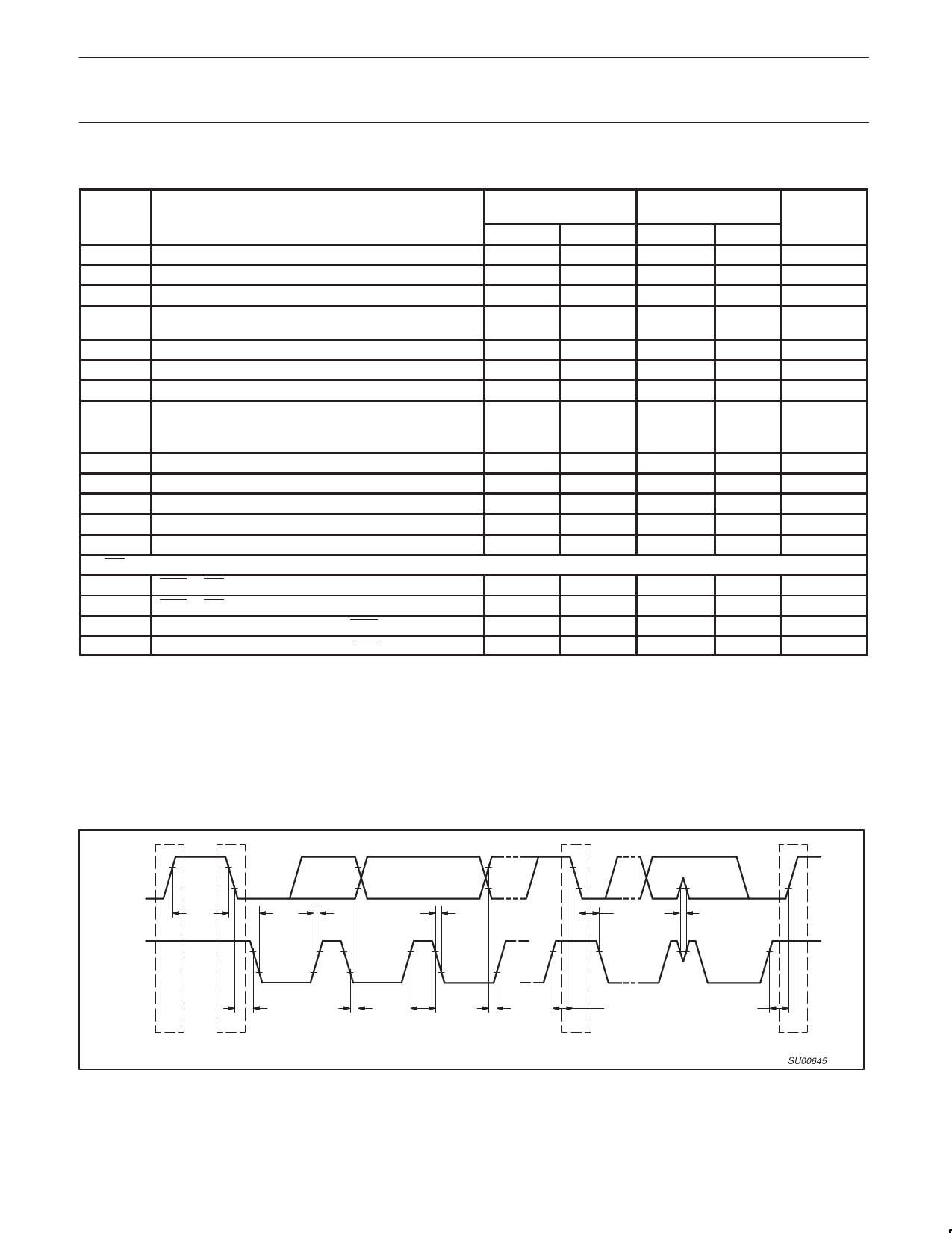
SDA
tBUF
tLOW
tR
tF
SCL
P
tHD;STA
S
tHD;DAT
tHIGH
tSU;DAT
tHD;STA
tSU;STA
Sr
Figure 8. Definition of timing on the I2C-bus
tSP
tSU;STO
P
SU00645
1999 Oct 07
8
Share Link: 